Fan Out Simple to Complex John Hunt
|
|
|
- Aubrie Shields
- 6 years ago
- Views:
Transcription

1 Fan Out Simple to Complex John Hunt Senior Director Engineering, Technical Promotion - ASE
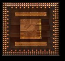
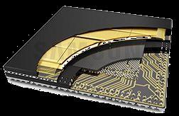
2 Package Focused Mechanical Processes Grinding Sawing Die Bonding Wire Bonding Molding Singulation + Wafer Focused + Chemical Processes Wafer Processing Sputtering Plating Etching Plasma Photo Processing Photoresists Polymers


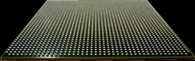
3 OSAT Wafer Mechanical Level Processing Bumping WLCSP

4 To Scale


5 Wafer Level Enabled New OSAT Packaging Bumping 2000 WLCSP 2001 Wafer Level Processing 2000 FOSiP 2017 FOPoP 2016 WL IPD 2005 HD Fanout 2014 WL MEMS 2008 WL Fan Out D Fan Out 2011


6 Fan In Package? Fan Out Package? Fan In All RDL traces are routed in towards the center of the die Fan Out RDL traces are routed both in and outwards beyond the limits of the die


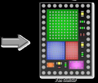

7 Drivers for Fan Out Die Shrinkage Fan Out allows ball placement beyond die area WLCSP FOWLP Heterogeneous & Homogeneous Integration Excellent electrical connectivity System in Package (SiP) Interconnect wide variety of components Small Size


8


9 Chip First Fan Out Chip First Fan Out Wafer Dicing Wafer Reconstitution Molding RDL Formation Backend Chip Last Fan Out Trace & Pad Formation Flip Chip & Molding Chip Last Fan Out Backend

 Fan")

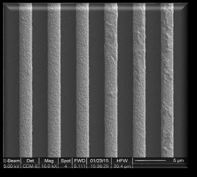
10 Low Density (LD) Fan Out Less than ~ I/O Lines/Spaces >= 8µm High Density (HD) Fan Out Greater than ~ I/O Lines/Spaces < 8µm


11 Low I/O, L/S >= 8µm Early Applications Baseband & RF Transceiver New Opportunities Varied Applications 24/77GHz Automotive Radar Automotive Medical PMIC mm Waveband Ultrasound DRAM & NAND Memory MEMS Sensors RF Connectivity NFC Chips WIFI Bluetooth GPS DC/DC Converters CODECS IPDs Audio Analog Touch IC Controllers LCD Display Drivers PA Modules
12 Chip First Die Down Chip First Die Up Chip Last (Panel) Chip Last (Wafer)


13 Single Die FOWLP Multi Die 2D Double sided 3D FOWLP PoP Multi Die 2D with Passives


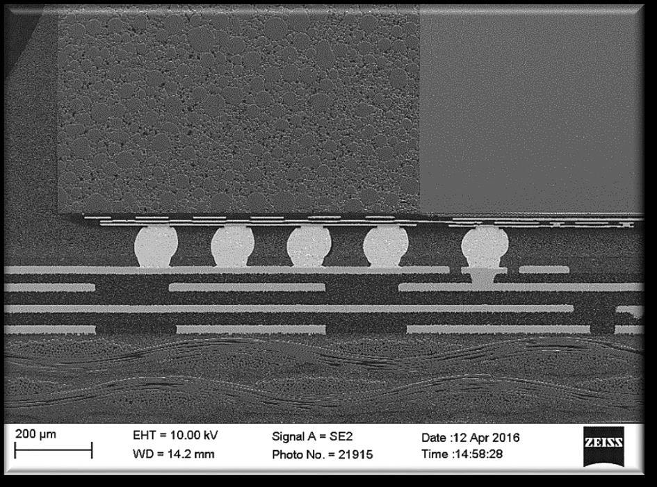
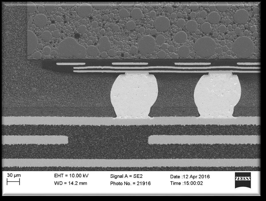
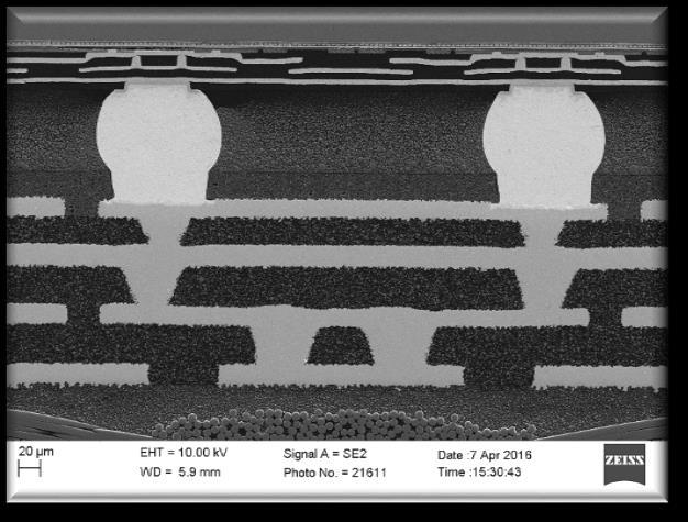
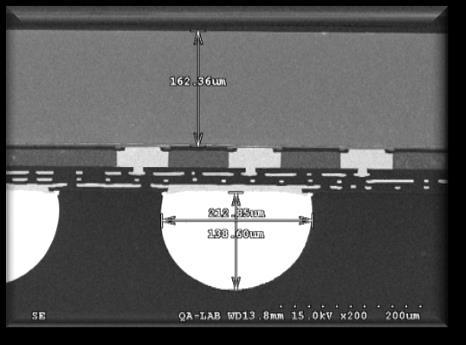
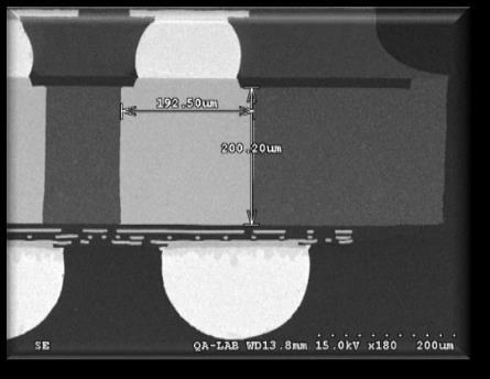
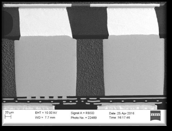
14 Mold compound allows additional spacing between the die and RDL traces & UBM and potentially better high frequency electrical performance Mold compound over die provides better buffering for Chip Package Interaction Chip First Die Down ewlb Chip First Die Up Deca M-Series M-Series Has 5X larger Standoff vs ewlb Drawings are shown to scale 14


15 HD Fan Out Opportunities High I/O, L/S <8µm Package on Package Applications (POP) System in Package Applications (SiP) Opportunities Varied Applications APU + Memory GPU + Memory Network Applications SiP/ Modules 15


16 HD Wafer Level Fan Out Variations Chip First Die Down HD ewlb FOCoS Hybrid Fan Out Chip on Substrate (FO FCBGA) Chip First Die Up HD FO HD FOPoP HD FOPoP with RDL HD FOPoP SiP Chip Last Chip Last Single Sided SiP Chip Last Double Sided PoP SiP Chip Last Double Sided PoP SiP w/rdl 16

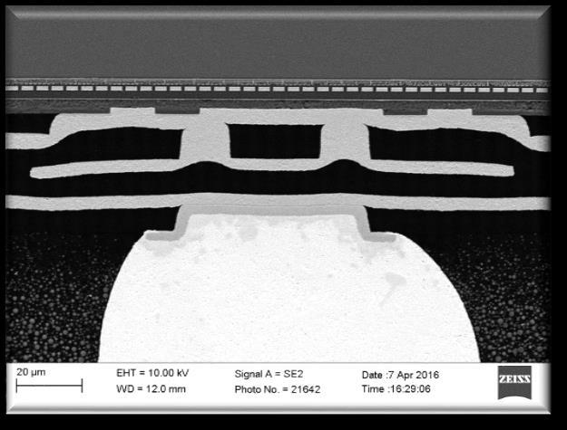
17 FOCoS Fan Out Chip on Substrate


18 High Density 2.1D Fanout 2.5D Alternative Organic 2.1D Interposer Applications APU + Memory GPU + Memory Network Applications SiP/ Modules Hybrid Solution Combines HD Fan Out with FCBGA High Density 2D & 3D Interconnection in RDL Layers, no need for interposer Most Complex Fan Out in Production Requires Advanced Fan Out & Advanced FlipChip Assembly Fan Out Compound Die Fan Out Hybrid BGA Package 2/2.5µm L/S 3 RDL Layers + UBM 16 & 28nm Die 24x26mm FO 45x45mm Package


19 FO on Substrate can Replace 2.5D

20 FOCoS Variations FOCoS Chip First Die Down FOCoS Chip Last 20

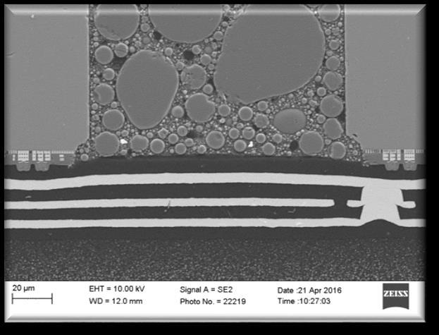
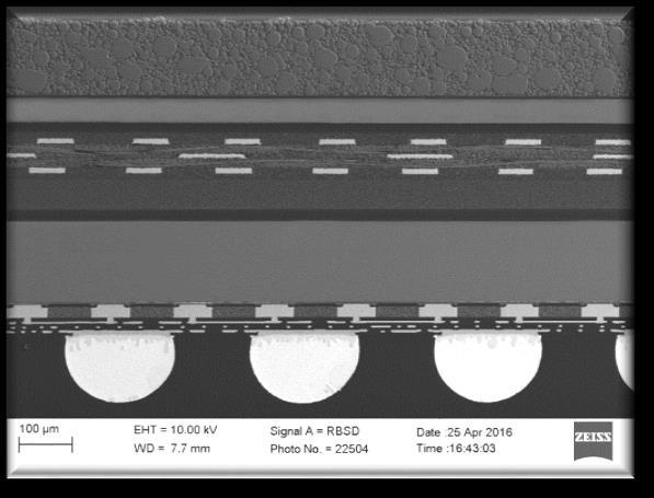
21 FOCoS in Production 2µ Line/2.5µ Space
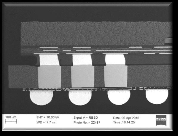
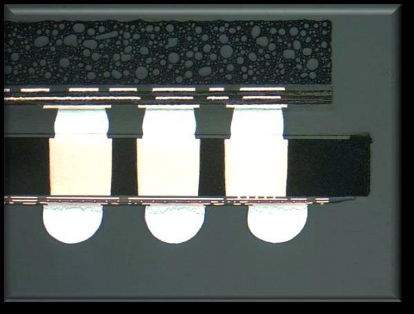
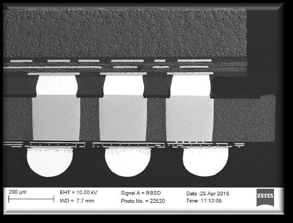
22 FOCoS Production Cross Sections
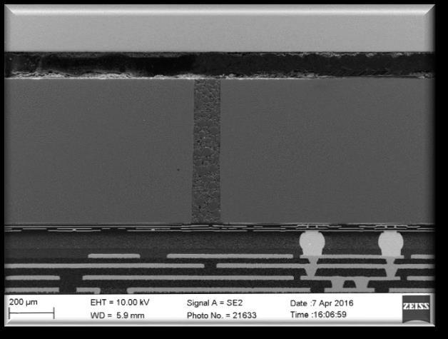
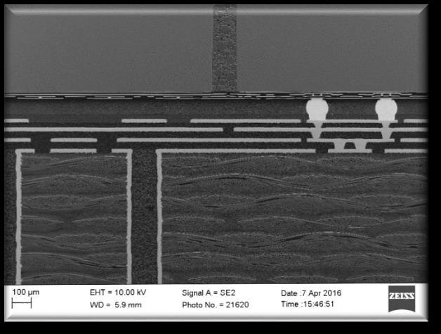
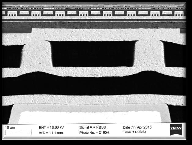
23 FOCoS Production Cross Sections


24 3D Fan Out Logic Bottom Package + Memory Package = Assembled Fan Out POP 24


25 Fan Out PoP

26 Fan Out POP
27 Chip Last Single Sided SiP Chip Last Double Sided POP SiP Chip Last Double Sided POP SiP w/rdl


28 In Production Eng/Qual BB, RF, Codec, PMIC, Car Radar. ewlb BB, RF, Codec, PMIC.. FOCLP BB, RF, Codec, PMIC.. FOCoS Fan Out Chip on Substrate Networking, Server.. M-Series BB, RF, Codec, PMIC.. FOPoP AP & Memory Integration.. FOSiP AP & Memory Integration, RF Module.. Max. Pkg size ~12x12 RDL L/S > 8/8um 2L RDL Production 180+M units shipped Since Y2009 Max. Pkg size ~12x12 RDL L/S > 12/12um 2L RDL Production 100M+ units shipped Since Y2014 Max. Pkg size ~45x45 RDL L/S => 2/2um 3L RDL, 4 Metal Production >800K units shipped Since Jan 2016 Max. Pkg size ~12x12 RDL L/S > 8/8um 2L RDL MultiDie Qualification Engineering Max. Pkg size ~15x15 RDL L/S => 5/5um 3L RDL Engineering Hundreds built, In Qualification Max. Pkg size ~15x15 RDL L/S => 5/5um 3L RDL Engineering Hundreds built Chip first - Wafer Die down Original FO in volume production Low & Medium Density I/O Multi-Die & Passives Chip last - Panel Cu pillar on die Very thin Coreless substrate Multi die + Passives Same form factor as ewlb Chip first - Wafer Die down Hybrid Fan Out Bumped pseudo-die ~12,000 I/O FC BGA Assembly Die to Die >1000 I/O Alternative to 2.5D Multi-Die & Passives Chip first - Wafer Die Up Deca Process Low & Medium Density I/O Multi-Die Wafer Panel Development Chip first/last - Wafer Die up Cu pillar on die Lowest PoP height High Bandwidth performance Multi-Die & Passives Chip last Wafer FO Known good RDL Die shift/warpage controlled High cure dielectric available Multi-Die & Passives


29 Fan In to Fan Out 2D to 3D ewlp FO Die Down M-Series FO Die Up Panel FO Chip Last Chip Last FO SiP Hybrid FO/BGA Die Down FO POP w/o Top RDL WLCSP FO POP w/top RDL FO POP w Memory FO Chip Last w/o Top RDL FO Chip Last w/top RDL


30 Summary New Packaging Innovations improve Cost Miniaturization Performance SiP WLCSP Fan Out Package 3D Fan Out Package on Package 3D FO System in Package 30
Stacked Die Advanced Interconnect Technologies
 Orient Semiconductor Electronics, Inc. OSE-USA Stacked Die Advanced Interconnect Technologies Dave Tovar VP of Technology Development OSE-USA Page: 1 Overview Summary Stacked Die Trends Challenges Wafer
Infrastructure for Rapid Assessment of Reliability
 Infrastructure for Rapid Assessment of Reliability Infrastructure and process improvements in the reliability testing of a high density microelectronic packaging technology Hannah Varner Draper Outline
MULTICHIP MODULE TECHNOLOGY HANDBOOK
 MULTICHIP MODULE TECHNOLOGY HANDBOOK Philip E. Garrou Dow Chemical Company IwonaTurlik Motorola McGRAW-HILL New York San Francisco Washington, D.C. Auckland Bogota Caracas Lisbon London Madrid Mexico City
Low Temperature Curable Polyimide Film Properties and WLP Reliability Performance with Various Curing Conditions
 2017 IEEE 67th Electronic Components and Technology Conference Low Temperature Curable Polyimide Film Properties and WLP Reliability Performance with Various Curing Conditions Yu Chuan Chen (Steven), Katch
Unified Padring Design Flow
 2013 First International Conference on Artificial Intelligence, Modelling & Simulation Unified Padring Design Flow Ang Boon Chong, Ho Kah Chun PMC-Sierra, Design Service, Penang,Malaysia Boonchong.ang@pmcs.com,
3D TSV Cu Pillar Probing Challenges & Experience
 3D TSV Cu Pillar Probing Challenges & Experience Ray Grimm/Mohamed Hegazy SV TCL An SV Probe Company Linjianjun (David) Hi Silicon Rick Chen SPIL The Challenges 2 Cu Pillar Bump Reliability Shear Test
Cu/SnAg Double Bump Flip Chip Assembly as an Alternative of Solder Flip Chip on Organic Substrates for Fine Pitch Applications
 Cu/SnAg Double Bump Flip Chip Assembly as an Alternative of Solder Flip Chip on Organic Substrates for Fine Pitch Applications Ho-Young Son 1), Gi-Jo Jung 2), Jun-Kyu Lee 2), Joon-Young Choi 2), and Kyung-Wook
Technology Challenges for Active Cardiac Implantable Devices. Alain Ripart Senior VP and CSO
 Technology Challenges for Active Cardiac Implantable Devices Alain Ripart Senior VP and CSO Heart rhythm disorders and associated therapy devices Bradycardia Pacemaker Atrial Arrhythmias Pacemaker Ventricular
Introducing Via-in-Pad Blind Via Technology to Any PCB Multilayer Fabricator
 Introducing Via-in-Pad Blind Via Technology to Any PCB Multilayer Fabricator Page 1 of 5 Larry W. Burgess MicroPak Laboratories, Inc. Wilsonville, OR 97070-1310 Abstract Via in Pad Blind Via Technology
Study of Micro-Electrode Array for Neural Populations Stimulating and Recording
 Study of Micro-Electrode Array for Neural Populations Stimulating and Recording Xiaoying Lü 1, Zhi-Gong Wang 2 1 State Key Lab of Bioelectronics 2 Institute of RF- & OE-Ics Southeast University, 210096
Electronic Packaging Moisture Interaction Study
 Electronic Packaging Moisture Interaction Study Yung Hsiang Lee, Ian Chin, Wei Keat Loh Intel Technology Sdn. Bhd. Lot 8, Jalan Hi-tech 2/3, Kulim Hi-tech Park, 09000 Kulim, Kedah, Malaysia yung.hsiang.lee@intel.com,
DATE 2006 Session 5B: Timing and Noise Analysis
 DATE 2006 Session 5B: Timing and Noise Analysis Bus Stuttering : An Encoding Technique To Reduce Inductive Noise In Off-Chip Data Transmission Authors: Brock J. LaMeres, Agilent Technologies Sunil P. Khatri,
SCS ELECTRONICS COATINGS. Reliable protection for advanced electronics.
 SCS ELECTRONICS COATINGS Reliable protection for advanced electronics. INNOVATIVE SOLUTIONS FROM THE LEADER IN PARYLENE With over 45 years of experience in Parylene engineering and applications, Specialty
STUDY ON APPLICATION OF STRAIN MEASURING TECHNOLOGY IN BOARD LEVEL ASSEMBLY PROCESS
 As originally published in the SMTA Proceedings STUDY ON APPLICATION OF STRAIN MEASURING TECHNOLOGY IN BOARD LEVEL ASSEMBLY PROCESS Yabing Zou, Daojun Luo, Weiming Li China Electronic Product Reliability
IPC-6018A. Microwave End Product Board Inspection and Test IPC-6018A. A standard developed by IPC. Supersedes IPC-6018 January 1998
 ASSOCIATION CONNECTING ELECTRONICS INDUSTRIES Microwave End Product Board Inspection and Test January 2002 A standard developed by IPC Supersedes IPC-6018 January 1998 2215 Sanders Road, Northbrook, IL
Optimization of MicroSpring Contact Design Parameters for Low Pressure Probing. Rod Martens, Larry Levy Southwest Test Workshop 2004
 Optimization of MicroSpring Contact Design Parameters for Low Pressure Probing Rod Martens, Larry Levy Southwest Test Workshop 2004 Contents Industry Driven Probing Requirements Probing Operating Space
Hydrogen-Sensing Characteristics of Palladium-Doped Zinc-Oxide Nanostructures
 Hydrogen-Sensing Characteristics of Palladium-Doped Zinc-Oxide Nanostructures Undergraduate Researcher Saranya Sathananthan University of Tennessee, Knoxville Faculty Mentor Vinayak P. Dravid Department
A hybrid concept as a new approach for the micro-production of magnetic actuators
 1 A hybrid concept as a new approach for the micro-production of magnetic actuators Rissing, L. H. H.; Creutzburg, T.; Steffens, M.; Reuter, G.; Lenarz, T. ABSTRACT Actuators that are widely used in industrial
SMART ACTIVE IMPLANTABLE MEDICAL DEVICES: A VISION FOR THE FUTURE
 SMART ACTIVE IMPLANTABLE MEDICAL DEVICES: A VISION FOR THE FUTURE Alain Ripart Senior Scientific Advisor Sorin Group September 27, 2012 Personalized medicine delivered by implanted devices is exploding
Investigation of Cu and Ni Diffusion Amounts for Silicon Substrates
 Investigation of Cu and Ni Diffusion Amounts for Silicon Substrates Sales Engineering dept. Abstract An investigation regarding the Cu and Ni diffusion amounts for silicon substrates was conducted. A Cu
Avoiding the Pitfalls of Voiding in PCB Assemblies. Kim Flanagan Indium Corporation SMTA Capital August 23 rd, 2018
 Avoiding the Pitfalls of Voiding in PCB Assemblies Kim Flanagan Indium Corporation SMTA Capital August 23 rd, 2018 Overview I. What is Voiding i. Causes I. Key Factors to Consider i. Symptom or Defect
A 2.4 GHZ FULLY INTEGRATED LC VCO DESIGN USING 130 NM CMOS TECHNOLOGY
 A 2.4 GHZ FULLY INTEGRATED LC VCO DESIGN USING 130 NM CMOS TECHNOLOGY Gaurav Haramkar 1, Prof. Rohita P. Patil 2 and Renuka Andankar 3 1 Department of E&TC Engineering, SKNCOE, University of Pune, Pune,
Mechanical Simulation of Probing on SMART POWER POA devices
 Luca Cecchetto STMicroelectronics Mechanical Simulation of Probing on SMART POWER POA devices June 8 to 11, 2008 San Diego, CA USA Authors L. Cecchetto, L. Zullino, R. Vallauri, L. Cerati, A. Andreini
Supporting Information. Comparing embodied greenhouse gas emissions of modern computing and electronics products. Paul Teehan, Milind Kandlikar
 Supporting Information Comparing embodied greenhouse gas emissions of modern computing and electronics products Paul Teehan, Milind Kandlikar This document contains 95 pages, one figure, and 42 tables.
Qualification and Performance Specification for Rigid Printed Boards
 Qualification and Performance Specification for Rigid Printed Boards Developed by the Rigid Printed Board Performance Specifications Task Group (D-33a) of the Rigid Printed Board Committee (D-30) of IPC
Defect Reduction Progress in Step and Flash Imprint Lithography
 Defect Reduction Progress in Step and Flash Imprint Lithography Kosta Selinidis, John G. Maltabes, Ian McMackin, Joseph Perez, Douglas J. Resnick, and S. V. Sreenivasan BACUS 2007 Introduction The purpose
get fitter faster Whatever your goal, stay motivated, have fun and train for success with micoach
 get fitter faster Whatever your goal, stay motivated, have fun and train for success with micoach OVERVIEW micoach is an interactive training service for anyone who wants to train for their favorite sport,
Solutions to Technical Challenges for WLBI Steve Steps
 Solutions to Technical Challenges for WLBI Steve Steps Major Technical Challenges Only three major challenges Thermal Mechanical Electrical June 9, 2002, Page 2 Major Thermal Challenges Adding heat or
Assembly Instruction for Fiber Optic Series FOH Fischer Connectors
 Assembly Instruction for Fiber Optic Series FOH Fischer Connectors Table des matières 1 Introduction... 3 2 Document history... 3 3 Definitions and Acronyms... 3 4 FOH Plugs & Receptacles with Potting
PZT/ZnO EXPERIMENT MODELLING
 Mat. Res. Soc. Symp. Proc. Vol. 655 2001 Materials Research Society High Frequency Thin Film Acoustic Ferroelectric Resonators Paul Kirby a, Qing-Xin Su a, Eiju Komuro b, Masaaki Imura b, Qi Zhang, and
Interconnect Manufacturing Challenges for the Most Advanced Technology Nodes
 Interconnect Manufacturing Challenges for the Most Advanced Technology Nodes Andrzej J. Strojwas Chief Technologist, PDF Solutions, Inc., San Jose, CA Keithley Professor of ECE, Carnegie Mellon University,
?Cl-\-e~+ J:l 0 t q;its -'{
 ?Cl-\-e~+ J:l 0 t q;its -'{ f:lj.tt ~ J:,LJ ct{ lcfctc( :r::~~~-(j F.et; ('S"JOO 1 Reusable Wafer Support for Semiconductor Processing Ia. GENERAL PURPOSE This invention provides a reusable support for
Materials Declaration Form
 Materials Declaration Form IPC 1752 Version 2 Form Type * Distribute Sectionals * Material Info Subsectionals * A-D Manufacturing Info * : Required Field Supplier Information Company Name * STMicroelectronics
Patterned Wafer Defect Density Analysis of Step and Flash Imprint Lithography
 Patterned Wafer Defect Density Analysis of Step and Flash Imprint Lithography I. McMackin, W. Martin, J. Perez, K. Selinidis, J. Maltabes, F. Xu, D. Resnick, SV Sreenivasan EIPBN 2007 Introduction The
Mike Davies Director, Neuromorphic Computing Lab Intel Labs
 Mike Davies Director, Neuromorphic Computing Lab Intel Labs Loihi at a Glance Key Properties Integrated Memory + Compute Neuromorphic Architecture 128 neuromorphic cores supporting up to 128k neurons and
5GHz Band SPDT Switch + LNA GaAs MMIC
 5GHz Band SPDT Switch + LNA GaAs MMIC GENERAL DESCRIPTION The NJG1739K51 is a 5GHz band SPDT switch + low noise amplifier GaAs MMIC designed for wireless LAN front-end applications. The NJG1739K51 features
Multi-band LC VCO GHz PMCC_VCOMB12G
 Multi-band LC VCO 8-11.3GHz PMCC_VCOMB12G IP MACRO Datasheet Rev 1.2 Process: 65nm CMOS DESCRIPTION PMCC_VCOMB12G is a low noise multi-band differential LC voltage controlled oscillator (VCO). The IP block
Bio Compatible Microsystem Packaging of VCSELaser for Implantable Devices
 Bio Compatible Microsystem Packaging of VCSELaser for Implantable Devices Dr Alexander Steinecker, CSEM, Alpnach (CH) EPoSS Annual Forum, Torino (IT), 25.09.2014 Copyright 2014 CSEM Alexander Steinecker
Impact of Local Interconnects on Timing and Power in a High Performance Microprocessor
 Impact of Local Interconnects on Timing and Power in a High Performance Microprocessor Rupesh S. Shelar Low Power IA Group Intel Corporation, Austin, TX December 13 th 2011 UT ICS/IEEE Seminar, UT Austin
Modelling and Fabrication of High Frequency Ultrasound Transducer Arrays for Medical Applications
 Modelling and Fabrication of High Frequency Ultrasound Transducer Arrays for Medical Applications Robert T. Ssekitoleko DTC in Medical Devices, University of Strathclyde Gerry Harvey Weildlinger Associates,
Effects of Zn-Bearing Flux on Joint Reliability and Microstructure of Sn-3.5Ag Soldering on Electroless Ni-Au Surface Finish
 Materials Transactions, Vol. 51, No. 10 (2010) pp. 1727 to 1734 Special Issue on Lead-Free and Advanced Interconnection Materials for Electronics #2010 The Japan Institute of Metals Effects of Zn-Bearing
Electrical Contact Resistance - The Key Parameter in Probe Card Performance
 January Kister Steve Hopkins MicroProbe, Inc. Electrical Contact Resistance - The Key Parameter in Probe Card Performance 2007 San Diego, CA USA Overview Test cell & Contact Resistance measurement system
High Frequency Piezo Composites Microfabricated Ultrasound Transducers for Intravascular Imaging
 High Frequency Piezo Composites Microfabricated Ultrasound Transducers for Intravascular Imaging Jian. R. Yuan 1, X. Jiang 2, l Pei-Jie Cao 1, 1 Boston Scientific Imaging, Fremont, CA Alain Sadaka 1, Rick
GLAST Large Area Telescope:
 Gamma-ray Large Area Space Telescope GLAST Large Area Telescope: Tracker Subsystem MCM Production Readiness Review MCM Design Overview Robert Johnson Santa Cruz Institute for Particle Physics University
Thin Film Interposer (TFI ) Probes in Production
 Probes in Production") Chris Sullivan, John Hagios, Steve Duda, Sally Francis IBM Systems & Technology Group Essex Junction, Vermont Thin Film Interposer (TFI ) Probes in Production Challenges, Experiences, and Lessons Learned
Chris Sullivan, John Hagios, Steve Duda, Sally Francis IBM Systems & Technology Group Essex Junction, Vermont Thin Film Interposer (TFI ) Probes in Production Challenges, Experiences, and Lessons Learned
Feasibility Study for: IEEE GbE Electrical Backplane / Copper Cabling Study Group. Fort Lauderdale, FLA. Vittal Balasubramanian
 Feasibility Study for: IEEE 8. GbE Electrical Backplane / Copper Cabling Study Group Fort Lauderdale, FLA Vittal Balasubramanian Signal Integrity Team January Purpose To show the possible reach that can
(Pd) 2.1 LCD 600. ( 1<cm 2 /V.s)[46] LCD. 40~150 cm 2 /Vs[47] [47]-[49]: PECVD ECRCVD 250 ~300. Phase Crystallization):
![(Pd) 2.1 LCD 600. ( 1<cm 2 /V.s)[46] LCD. 40~150 cm 2 /Vs[47] [47]-[49]: PECVD ECRCVD 250 ~300. Phase Crystallization):](/thumbs/88/116384449.jpg "(Pd) 2.1 LCD 600. ( 1<cm 2 /V.s)[46] LCD. 40~150 cm 2 /Vs[47] [47]-[49]: PECVD ECRCVD 250 ~300. Phase Crystallization):") (Pd) 2.1 LCD 600 ( 1
(Pd) 2.1 LCD 600 ( 1
G-Premio BOND. One component light cured universal adhesive. BOND with the BEST
 One component light cured universal adhesive BOND with the BEST The world s most clinically successful adhesive is now even better! Introducing. G-BOND has proven to be the world s most clinically successful
UV + PVD: PERFORMANCE AND DESIGN SOLUTIONS FOR THE AUTOMOTIVE INDUSTRY. Eileen M. Weber, Red Spot Paint and Varnish, Co., Inc.
 UV + PVD: PERFORMANCE AND DESIGN SOLUTIONS FOR THE AUTOMOTIVE INDUSTRY Eileen M. Weber, Red Spot Paint and Varnish, Co., Inc. What Is PVD? Physical Vapor Deposition PVD is deposition of a metal onto a
Valve-Based Microfluidic Compression Platform: Single Axon Injury and Regrowth
 Supplementary Material (ESI) for Lab on a Chip This Journal is The Royal Society of Chemistry 2011 Valve-Based Microfluidic Compression Platform: Single Axon Injury and Regrowth Suneil Hosmane a, Adam
Flip Chips and Acoustic Micro Imaging: An Overview of Past Applications, Present Status, And Roadmap for the Future
 Flip Chips and Acoustic Micro Imaging: An Overview of Past Applications, Present Status, And Roadmap for the Future Janet E. Semmens Sonoscan, Inc. 2149 E. Pratt Boulevard Elk Grove Village, IL 60007 USA
Materials Declaration Form
 Materials Declaration Form IPC 1752 Version 2 Form Type * Distribute Sectionals * Material Info Subsectionals * A-D Manufacturing Info * : Required Field Supplier Information Company Name * STMicroelectronics
Journal of Faculty of Engineering & Technology DESIGN AND IMPLEMENTATION OF A WEARABLE HEALTH DEVICE
 PAK BULLET TRAIN (PBT) JFET 22(2) (2015) 39-44 Journal of Faculty of Engineering & Technology journal homepage: www.pu.edu.pk/journals/index.php/jfet/index DESIGN AND IMPLEMENTATION OF A WEARABLE HEALTH
Human Energy Harvesting based on Piezoelectric Transduction using MEMS Technology
 Human Energy Harvesting based on Piezoelectric Transduction using MEMS Technology Queeni Sunder 1, Bakialakshmi 2 PG Student [E&C], Dept. of ICE, SRM University, Chennai, Tamilnadu, India 1 Assistant professor,
Pb-Free/RoHS Solutions
 Pb-Free/RoHS Solutions Environmental Policy: Exar Corporation is committed to protecting the environment and individual health and safety. We shall comply with all environmental regulations, health and
Section 1. Objective What is an electronic component? 2. What are passive and active components? 3. What are discrete components and ICs?
 Section 1 Objective 1 1. What is an electronic component? 2. What are passive and active components? 3. What are discrete components and ICs? DVD-64C v.1 Review Questions 1 Section 1 Objective 2 4. What
Controlling Contact Resistance with Probe Tip Shape and Cleaning Recipe Optimization
 SouthWest Test Workshop - 23 Controlling Contact Resistance with Probe Tip Shape and Cleaning Recipe Optimization Scott Stalnaker Clint Churchill Vail McBride Kelly Burnside AMI Semiconductor, Inc. 23
Les LEDs à Base de l Oxyde de Zinc D. Rogers : Nanovation & Universite de Technologie de Troyes F. Hosseini Teherani : Nanovation, France
 Les LEDs à Base de l Oxyde de Zinc D. Rogers : Nanovation & Universite de Technologie de Troyes F. Hosseini Teherani : Nanovation, France OUTLINE 1. Problems with Todays LEDs 2. ZnO vs GaN 3. Nanovation
QMTS2.E Polymeric Materials - Filament-wound Tubing, Industrial Laminat...
 QMS2.E199230 - Polymeric Materials - Filament-wound ubing, ndustrial Laminat... http://database.ul.com/cgi-bin/xyv/template/lsex/1frame/showpage.html?nam... Page 1 of 5 QMS2.E199230 Polymeric Materials
SUPPLEMENTARY INFORMATION
 Supporting Online Material High resolution electroluminescent imaging of pressure distribution using a piezoelectric nanowire-led array Caofeng Pan 1,2, Lin Dong 1,2, Guang Zhu 1, Simiao Niu 1, Ruomeng
Lecture 180 CMOS Technology (10/20/01) Page 180-1
 Page 180-1") Lecture 180 CMOS Technology (10/20/01) Page 180-1 LECTURE 180 CMOS TECHNOLOGY (READING: Text-Sec. 2.8) INTRODUCTION Objective The objective of this presentation is: 1.) Illustrate the fabrication sequence
Lecture 180 CMOS Technology (10/20/01) Page 180-1 LECTURE 180 CMOS TECHNOLOGY (READING: Text-Sec. 2.8) INTRODUCTION Objective The objective of this presentation is: 1.) Illustrate the fabrication sequence
Control of Spatial Uniformity in Microelectronics Manufacturing: An Integrated Approach
 Control of Spatial Uniformity in Microelectronics Manufacturing: An Integrated Approach H. Zhang & M. Nikolaou Chemical Engineering Department University of Houston Real-Time Feedback Control of Spatial
Shape Memory Alloy Micro-Actuator for Handling of Head Gimbal Assembly
 AIJSTPME (2011) 4(4): 1-8 Shape Memory Alloy Micro-Actuator for Handling of Head Gimbal Assembly Prapaipittayakhun K. Department of Mechanical Engineering, Faculty of Engineering, Chulalongkorn University,
PV wafer production Ideas for Low-cost-manufacturing for MONO, MULTI and MONO-Like PV-SOLAR-WAFER
 PV wafer production Ideas for Low-cost-manufacturing for MONO, MULTI and MONO-Like PV-SOLAR-WAFER Roadmap for big Wafer cost reduction MONO 60 to 30 cts. POLY 49 to 13 cts. Invention of Diamond-Wire by
Keylock switches for PCB
 lock switch for PCB General data lock switch for PCB mounting. Matching with the RS 76 full-travel keyswitch and the RF 15 and RF 19 short-travel keyswitch. Content lock switch IP5, MICROMEC - 18 lock
QS S Assist KINASE_ADP-Glo TM Kit
 QS S Assist KINASE_ADP-Glo TM Kit Description KINASE ADP-Glo TM kit is designed for use in biochemical kinase assays based on a Luminescent ADP Detection Assay (ADP-Glo TM ). The kit includes human kinase,
D-Mannitol Assay Kit (Colorimetric)
") D-Mannitol Assay Kit (Colorimetric) Catalog Number KA3760 100 assays Version: 02 Intended for research use only www.abnova.com Table of Contents Introduction... 3 Background... 3 General Information...
D-Mannitol Assay Kit (Colorimetric) Catalog Number KA3760 100 assays Version: 02 Intended for research use only www.abnova.com Table of Contents Introduction... 3 Background... 3 General Information...
TOTAL IONIZING DOSE RADIATION TEST REPORT RH3080
 TOTAL IONIZING DOSE RADIATION TEST REPORT RH3080 April 2018 Product: Total ionizing dose level: Source: Dose Rate: Facilities: Radiation Test Report RH3080 High dose rate: 200 krad(si) Low dose rate: 100
SiS9255. Projected Capacitive. Touch-Screen Micro Processor. Data sheet. Rev. 1.2 August 18, 2015
 SiS9255 Projected Capacitive Touch-Screen Micro Processor Data sheet Rev. 1.2 August 18, 2015 This specification is subject to change without notice. Silicon Integrated Systems Corporation assumes no responsibility
Cross-Interaction between Ni and Cu across Sn Layers with Different Thickness
 Journal of ELECTRONIC MATERIALS, Vol. 36, No. 11, 2007 DOI: 10.1007/s11664-007-0235-0 Ó 2007 TMS Special Issue Paper Cross-Interaction between Ni and Cu across Sn Layers with Different Thickness CHIEN
Path to High-Quality Films on Continuous Substrates
 Spatial Atomic Layer Deposition: A Path to High-Quality Films on Continuous Substrates t David H. Levy, Roger S. Kerr, Shelby F. Nelson, Lee W. Tutt, and Mitchell Burberry Eastman Kodak Company Rochester,
Thin-film barriers using transparent conducting oxides for organic light-emitting diodes
 Thin-film barriers using transparent conducting oxides for organic light-emitting diodes Ho Nyeon Lee Hyung Jung Kim Young Min Yoon Abstract This study covers thin-film barriers using inorganic barriers
MAKE SMART INJECTION CHOICES INJECTION PROVIDERS GUIDE FOR SAFE INJECTIONS
 MAKE SMART INJECTION CHOICES INJECTION PROVIDERS GUIDE FOR SAFE INJECTIONS MAKE SMART INJECTION CHOICES WHO recommends syringes with re-use prevention (RUP) features for all injections. RUP syringes with
Modeling the Array Force of C4 Probe Cards during Wafer Sort
 Modeling the Array Force of C4 Probe Cards during Wafer Sort Arun Ramamoorthy Intel Corporation 1 Overview! Problem Definition! System Model PCB Deflection Model Pro/E and Pro/Mechanica model Chuck Deflection!
Analog Design and System Integration Lab. Graduate Institute of Electronics Engineering National Taiwan University
 Designs of Low-Noise K-band K VCO Analog Design and System Integration Lab. Graduate Institute of Electronics Engineering National Taiwan University Introduction Outlines The proposed VCO architecture
Synthesis and Characterization of Mn 2+ Doped Zn 2. Phosphor Films by Combustion CVD Method
 Synthesis and Characterization of Mn 2+ Doped Zn 2 Phosphor Films by Combustion CVD Method Z. T. Kang a, Y. Liu b, B. K. Wagner a, R. Gilstrap a, M. Liu b, and C. J. Summers a a Phosphor Technology Center
Qingtian Instrument Kaifeng Qingtianweiye Flow Instrument Co.,Ltd
 Qingtian Instrument Kaifeng Qingtianweiye Flow Instrument Co.,Ltd Section One Company Profile 2 Kaifeng Qingtianweiye Flow instrument Co., Ltd was founded in 2005,located in China flow instrument production
Analyses of Intravesicular Exosomal Proteins Using a Nano-Plasmonic System
 Supporting Information Analyses of Intravesicular Exosomal Proteins Using a Nano-Plasmonic System Jongmin Park 1, Hyungsoon Im 1.2, Seonki Hong 1, Cesar M. Castro 1,3, Ralph Weissleder 1,4, Hakho Lee 1,2
Guidelines for surface adhesion with. marine DB50 SWISS MADE
 0575 Flächenverklebung mit Guidelines for surface adhesion with Merbenit DB50 DB50 Before starting the adhesion process, all assembly parts have to be prepared accordingly. The surface treatment of the
G-Premio BOND. Introducing a premium bonding experience
 Introducing a premium bonding experience The world s most clinically successful adhesive is now even better! Introducing G-Premio BOND. G-BOND has proven to be the world s most clinically successful adhesive
Deep Compression and EIE: Efficient Inference Engine on Compressed Deep Neural Network
 Deep Compression and EIE: Efficient Inference Engine on Deep Neural Network Song Han*, Xingyu Liu, Huizi Mao, Jing Pu, Ardavan Pedram, Mark Horowitz, Bill Dally Stanford University Our Prior Work: Deep
Interfacial bonding behavior with introduction of Sn Zn Bi paste to Sn Ag Cu ball grid array package during multiple reflows
 Interfacial bonding behavior with introduction of Sn Zn Bi paste to Sn Ag Cu ball grid array package during multiple reflows Po-Cheng Shih and Kwang-Lung Lin a) Department of Materials Science and Engineering,
Supplementary Information
 Electronic Supplementary Material (ESI) for ChemComm. This journal is The Royal Society of Chemistry 2015 Supplementary Information Comprehensive biosensor integrated with ZnO nanorods FETs array for selective
Research on Digital Testing System of Evaluating Characteristics for Ultrasonic Transducer
 Sensors & Transducers 2014 by IFSA Publishing, S. L. http://www.sensorsportal.com Research on Digital Testing System of Evaluating Characteristics for Ultrasonic Transducer Qin Yin, * Liang Heng, Peng-Fei
TECHNICAL UPDATE. Introducing SMA EP400 Resin and EP400S Resin Solution for Improved Copper Adhesion in Copper Clad Laminate BENEFITS.
 BENEFITS Excellent reactivity Improved adhesion to copper Non-tacky prepregs Multi-functional, effective crosslinker High chemical resistance TARGET MARKETS Copper Clad Laminates Structural Composites
The Custom Interconnect Leader
 QC Series 1.24 (31.5) 0.93 TYP (23.6) 0.180 (4.6) 0.413 (10.5) 0.112 (2.8) Figure 1: Standard 1.25" Mounting ELECTRICAL Nominal Impedance: Frequency Range: Voltage Rating: Dielectric Withstanding Voltage:
MSD P13038 Hearing Aid Design. Final Review May 10, 2013
 MSD P13038 Hearing Aid Design Final Review May 10, 2013 Agenda 5.10.13 Project Overview (2) Mechanical Needs & Spec Review (10) Electrical & Computer Needs & Spec Review (10) Budget Review (2) Schedule
Optical cochlear implant project
 Optical cochlear implant project Dr.-Ing. Stefan Mohrdiek MNBS 2014 LAAS, Toulouse 21 & 22 October 2014 This project is supported by the EU Commission, the European Research Funding organization under
AVR Based Gesture Vocalizer Using Speech Synthesizer IC
 AVR Based Gesture Vocalizer Using Speech Synthesizer IC Mr.M.V.N.R.P.kumar 1, Mr.Ashutosh Kumar 2, Ms. S.B.Arawandekar 3, Mr.A. A. Bhosale 4, Mr. R. L. Bhosale 5 Dept. Of E&TC, L.N.B.C.I.E.T. Raigaon,
LOCALISATION, IDENTIFICATION AND SEPARATION OF MOLECULES. Gilles Frache Materials Characterization Day October 14 th 2016
 LOCALISATION, IDENTIFICATION AND SEPARATION OF MOLECULES Gilles Frache Materials Characterization Day October 14 th 2016 1 MOLECULAR ANALYSES Which focus? LOCALIZATION of molecules by Mass Spectrometry
Technique Manual Technique Manual Rev. A 01/11/2011
 Technique Manual Technique Manual Table of Contents Introduction 4 Indications 5 Instrumentation 6 Frame Assembly 7 Position Guide 8-9 Tips and Tricks 10-13 Cleaning 14 Sterilization 14 Storage Instructions
Failure Mechanisms and Risk on LEDs and LED Systems SMT
 Failure Mechanisms and Risk on LEDs and LED Systems SMT 5.5. 07.05.2015 Zwolle Noerdlingen Stuttgart Dresden Bath Why is the life time limited? The LED chip has a proven life time of more than 50.000 hours
CATALOG OF REPLACEMENT PARTS
 CATALOG OF REPLACEMENT PARTS CC34, B32, & C32 FOOD PROCESSORS CC34 B32 C32 FORM 43143 Rev. B (May 2016) F-43143 Rev. B (May 2016) - 2-2016 Table of Contents 5 FEED HEAD AND HOUSING 7 ELECTRICAL COMPONENTS
Sign Language Interpretation Using Pseudo Glove
 Sign Language Interpretation Using Pseudo Glove Mukul Singh Kushwah, Manish Sharma, Kunal Jain and Anish Chopra Abstract The research work presented in this paper explores the ways in which, people who
Automatic Probe Assembly Machine
 Author: Dave Oh Kyung-hwan KIM Jung-pyo Chun (Presenter) TSE Co.,Ltd. Automatic Probe Assembly Machine June 8-11, 2008 San Diego, CA USA Table of Contents 1 st Section: Conventional Methods of Assembly
Set-up Instructions. MANUFACTURED BY COMMUNICATIONS-APPLIED TECHNOLOGY CO., INC. RESTON, VA. CAGE CODE: 0EEY2
 Set-up Instructions C-AT Level A/B Radio Interface with: Push-to-Talk Assembly, Shaped Audio Throat Microphone Bi-aural Speaker Assembly (two configurations) MANUFACTURED BY COMMUNICATIONS-APPLIED TECHNOLOGY
CETR Adhesion Testing on Glass/Al Surface for Corning Inc.
 CETR Adhesion Testing on Glass/Al Surface for Corning Inc. I. Introduction 1.1 Objective The goal of the study was to differentiate stiction from various glass composites and surface treatments using the
AND BIOMEDICAL SYSTEMS Rahul Sarpeshkar
 ULTRA-LOW-POWER LOW BIO-INSPIRED INSPIRED AND BIOMEDICAL SYSTEMS Rahul Sarpeshkar Research Lab of Electronics Massachusetts Institute of Technology Electrical Engineering and Computer Science FOE Talk
SCIENTIFIC PAPERS OF THE UNIVERSITY OF PARDUBICE THE CHARACTERIZATION OF ZINC PLATED SURFACES AFTER AGED ADHESİVES
 SCIENTIFIC PAPERS OF THE UNIVERSITY OF PARDUBICE Series B The Jan Perner Transport Faculty 19 (2014) THE CHARACTERIZATION OF ZINC PLATED SURFACES AFTER AGED ADHESİVES Alp ÖZDEMİR, Pavel ŠVANDA Department
Victory Series Active Self-Ligating Brackets. Reliable. and. Effective
 Victory Series Active Self-Ligating Brackets Reliable and Effective Victory Series Active Self-Ligating Brackets Reliability Victory Series SL Brackets are widely accepted as an industry benchmark for