SUPPLEMENTARY INFORMATION
|
|
|
- Chester Norman
- 5 years ago
- Views:
Transcription
1 Supporting Online Material High resolution electroluminescent imaging of pressure distribution using a piezoelectric nanowire-led array Caofeng Pan 1,2, Lin Dong 1,2, Guang Zhu 1, Simiao Niu 1, Ruomeng Yu 1, Qing Yang 1, Ying Liu 1, Zhong Lin Wang 1,2 * 1. School of Materials Science and Engineering, Georgia Institute of Technology, Atlanta, GA , USA 2. Beijing Institute of Nanoenergy and Nanosystems, Chinese Academy of Sciences, Beijing, , P.R. China *To whom the correspondence should be addressed. zhong.wang@mse.gatech.edu Contents: A: Experiment set-up and measurement system B: FEM modeling of basic mechanics and physics C: Devices fabrication process and hydrothermal growth of nanowires D: I-V characterization and electroluminescence images of nano-leds array E: Repeatability test and reversible experiments F: More High-spatial resolution pressure images G: Novel designs for the feasibility to extend the current approach to soft substrates NATURE PHOTONICS 1
 with closed loop resolution 0.2 nm, as shown in Fig. S1.")
2 A: Experiment set-up and measurement system The measurement system was built based on an inverted microscope (Nikon Ti-E), 3D micromanipulation stages and a piezo nanopositioning stage (PI, P-753K078) with closed loop resolution 0.2 nm, as shown in Fig. S1. A normal force/pressure was applied on the NW LEDs by using a sapphire substrate with a convex character pattern of PIEZO molded on it at the first place. By controlling the 3D micromanipulation stages and the piezo nanopositioning stage, the pressure could be applied step by step at a fixed value. The detailed calculation of the strain in ZnO NWs can be found in the support information of our previously work 1. The output light emission images were recorded by CCD and the electroluminescence spectra were recorded using a fiber optical spectrometer (Master Systems Felix32 PTI). We monitored the pressure change from the light emitting intensity change with image acquisition and processing technologies. 2 NATURE PHOTONICS
3 SUPPLEMENTARY INFORMATION Figure S1 Schematic diagram of the measurement system for characterizing the performance of a ZnO nanowire LEDs under applied compressive strain. B: FEM modeling of basic mechanics and performance of the device To carry out a systematical study about the device s performace, we build a FEM modeling using COMOSOL (version 4.2a) and studied the device response based on models conducted with different geometry (NWs diameter, NWs length, NWs spacing), different material properties (Young s modulus, substrate thickness and modulus). All of the parameters of the structure layouts in the FEM modeling are the same as for practical devices. Some design rules are derived through this systematical FEM modeling for achieving optimum performance. B1. Several design rules derived from FEM modeling We have carried out a systematically FEM modeling of the device response, as presented in the next few subsections, for different NW geometry (diameters and length), NW spacing, matrix modulus, substrate thickness and modulus. Based on the numerical calculations, several design rules are derived as summarized as follows: (1) The device is very uniform, the distribution of stress and strain in the ZnO NWs are very uniform over 99.7% for a 2cm*2cm device used in our experiment, only the 30 μm at the edge zone is not very uniform (Fig. S2 and S3) (2) The length of ZnO NWs is not very important for the device when the length is less than 25 μm, which approaches the limitation of the NW length fabricated by hydrothermal methods. (Fig. S4) (3) Spacing is very important for the device, and there is an optimum spacing when the diameter of the NWs is fixed. For NWs with diameter about 1.5 μm, the best spacing is 8 μm. (Fig. S5) (4) The diameter of ZnO NW is very important to the performance of the device. Small diameter would have good response and good sensitivity. Ideally, we will try to use small diameter ZnO NWs, such as 100 nm. However, by considering the fabrication cost and the device performance, 1 μm is a good choice. (Fig. S6) (5) For the matrix materials, it is better to use the one with smaller modulus. By considering the electronic property, and micro-fabrication related issues, PMMA and BCB are two best choices. (Fig. S7) (6) Thickness and modulus of the substrate are not important for our common substrates, such as sapphire and silicon wafers. By considering the ZnO NW growth condition and the LED technology, sapphire is the best choice for our experiment. (Fig. S8 and S9) (7) A tiny fluctuation (e.g. 1-2%) in the length of NWs does not affect the sensing result after depositing the top ITO electrode and the packaging layer, because the large deformation of the ITO and packaging layer due to their low young s modulus will tolerate the small variation in NW lengths (Fig. S10) B2. Distribution of strain and stress in the device for different nanowire dimensions. As shown in Fig. S2, 51 ZnO NWs array were built on a GaN/Sapphire substrate, the matrix is PMMA as we used in the experiments, and a layer of 300 nm ITO layer is on top of the composite structure. At last, a layer of 5 μm PDMS is on the top most of the structure. There are two reasons for introducing the NATURE PHOTONICS 3
4 PDMS layer, one is to serve as the package layer, and the other is the convex character pattern of PIEZO made by polymer (SU-8), where the stress was applied to. The dimensions of each component are as following: Sapphire substrate: thickness = 20 μm (this thickness will NOT affect the performance of the device, see Fig. S8) ZnO NWs: diameter = 1.5 μm, length = 3.8 μm (the average in our experiments) ZnO NW spacing: 4 μm (the center to center distance between two adjacent ZnO NWs) PMMA: 2.5 μm by 3.8 μm ITO top electrode: 300 nm PDMS layer: 5 μm After a uniform stress of 0.8 GPa is applied on the surface of the device, the stress distribution in the devices is shown in Fig. S2a. Due to the limitation of our computation power, we only built 51 NWs on the substrate in this modeling, it is clearly that the stress distribution in ZnO NWs is very uniform over the central 200 μm (see the enlarged result in Fig. S2b and Fig. S2c), except the four ZnO NWs at the edges, which is only less than 20 μm, as shown in Fig. S2a. For the devices used in the test, the size is about 2 cm by 2 cm, the response of NWs of the device can be treated as very uniform if we build the strain sensor on the center part of the whole device, not at the 100 μm edge area. To further confirm the uniformity of stress in ZnO NWs, we extract the stress profile at the interface between n-zno and p-gan, where the light emit, and shown in Fig. S3c and Fig. S3d. we can find that the stress in ZnO NW is very uniform and is about 1.7GPa (Fig. S3c); the strain in ZnO is also very uniform, which is near 1.0% (Fig. S3d). 4 NATURE PHOTONICS

5 SUPPLEMENTARY INFORMATION Figure S2 FEM modeling shows the distribution of stress in the device. a, A low-magnification view of the device. b-c, Enlarged view of the device, indicating that the stress is uniform in the middle of the device. d, The stress in a single ZnO NW, and the scale bar of stress, which unit is Pa. NATURE PHOTONICS 5

6 Figure S3 a, The stress distribution in the device. b, The strain distribution in the device. c, The 1D cut profile of the stress at the interface between ZnO and GaN. d, The corresponding 1D cut profile of the strain at the interface between ZnO and GaN. B3. Effect of NW diameter, length and spacing on device performance As shown in Fig. S4, three different NW lengths are used in the FEM modeling, 3.8 μm, 15 μm and 25 μm. The results of the NWs with length 3.8 μm and 15 μm are shown in Fig. S4a and S4b, and the 1D cut profile of stress and strain at the interface between ZnO and GaN is extracted and presented in Fig. S4d and S4e. We can reach the conclusion from the line profile that the length of the ZnO NWs DOES NOT affect the stress and strain distribution in ZnO NWs, which decides the performance of the device; it will only change the stress and strain distribution in the matrix (PMMA), which will not have impact on the performance of the device and the intensity of LEDs. 6 NATURE PHOTONICS

7 SUPPLEMENTARY INFORMATION Figure S4 The FEM modeling results showing the stress and strain distribution depending on the length of NWs. a, The length of ZnO NW is 3.8 μm. b, The length of ZnO NW is15 μm. c, The stress in an individual ZnO NW. d-e, The 1D cut profile of stress and strain at the interface between ZnO and GaN. The spacing effect was modeled with all other parameters being fixed, and the results are shown in Fig. S5. Here we define spacing as the NW center to center distance. We set the spacing as 4 μm, 6 μm, 8 μm, 10 μm and 12 μm, and three of them are shown in Fig. S5a (4 μm), Fig. S5b (8 μm), and Fig. S5c (12 μm). The line profile of the stress at the interface between ZnO NW and GaN film is shown in Fig. S5d. There exists an optimum spacing value for the sensitivity of the device; the stress is larger at the root of ZnO NWs in case of the spacing of 8 μm than that of spacing 4 μm and 12 μm, when an external stress about 0.8 GPa is applied on the surface of the device as shown in Fig. S5c. The plots of the stress at the root of ZnO NW and the PMMA versus the spacing are presented in Fig. S5e. At the beginning, the stress in the ZnO increases when the spacing increases. This is because the density of ZnO NW decreases, so the stress in each NW increases. When the spacing continues to increase, the stress in the ZnO NW begins to decrease when the spacing is over 8 μm (see the blue plot in Fig. S5e). This is because a part of the external stress was applied on the PMMA matrix, which is approved by the FEM modeling result shown in Fig. S5e, red line. We can see that the stress in the PMMA increases with increasing the spacing. We can reach a conclusion that an optimum spacing exists for our device, 8 μm is the best spacing for the device with NWs of diameter 1.5 μm, which was used in our experiment and this FEM modeling. NATURE PHOTONICS 7
.")
8 Figure S5 The FEM modeling results showing the stress distribution depends on the spacing of NWs. a-c, The spacing of the NWs is 4 μm, 8 μm and 12 μm, respectively. d, The 1D cut profile of stress at the interface between ZnO and GaN, when the devices have different spacings, the data were extracted from (a-c). e, The maximum stress in the root of ZnO NW (blue) and PMMA (red) versus different spacings. The relationship between the NW diameter and the device sensitivity was carried out with the FEM modeling as well. All other parameters are fixed except the NW diameter, and the results are shown in Fig. S6. Three typical FEM modeling results are shown in Fig. S6a (diameter 0.5 μm), Fig. S6b (diameter 1.5 μm) and Fig. S6c (2.5 μm), which obviously shows higher stress in the device with smaller diameter NWs. And the 1D cut profile of stress at the interface between ZnO and GaN are extracted and presented in Fig. S6d. Fig. S6e shows the relationship between the NW diameter and the stress in the ZnO NW. These results indicate that, the smaller the NW diameter is, the higher stress in the ZnO NW, which means the intensity of the LED is brighter, and better sensitivity of the devices will be obtained. However, in the fabrication process, there are several limitations for growth small diameter ZnO NWs. First, a photoresist layer with patterned pore diameter about nm was prepared by photolithography (PL), 8 NATURE PHOTONICS
, we can reach NW diameter about 200-300 nm or even less than this, as reported by us previously (Adv. Mater. 10, 22(42), 4749).")
9 SUPPLEMENTARY INFORMATION which makes the NW diameter around 1 μm. If we choose electron beam lithography (EBL), we can reach NW diameter about nm or even less than this, as reported by us previously (Adv. Mater. 10, 22(42), 4749). Based on considering the cost and the device performance, the diameter used in our experiment is around μm. Figure S6 The relationship between the NW diameter and the device sensitivity. Three typical diameter (a) 0.5 μm, (b) 1.5 μm, (c) 2.5 μm. d, 1D cut profile of stress at the interface between ZnO and GaN. e, Relationship between the NW diameter and the stress in the ZnO NW. B4. Effect of the modulus of the matrix material The modulus of the matrix material was studied with the FEM modeling, two kinds of frequently used matrix materials, PMMA (modulus 3 GPa, see Fig. S7b) and Benzocyclobutene (BCB, modulus 3.2 GPa), two other hypothetical matrix materials with modulus 1GPa (Fig. S7a) and 10 GPa (Fig. S7c) are used for the simulation, all other parameters are fixed, and the results are shown in Fig. S7. We can found that the stress in ZnO NW decrease when the matrix modulus increases, which means the sensitivity of the LED devices decreases with increasing the matrix modulus (Fig. S7d-e). NATURE PHOTONICS 9
, 3 GPa (b) and 10 GPa (c), respectively.")
10 Figure S7 The FEM modeling results showing the stress distribution depends on the modulus of matrix. a-c, The stress distribution depends on the modulus of matrix, with matrix modulus 1 GPa (a), 3 GPa (b) and 10 GPa (c), respectively. d, The 1D cut profile of stress at the interface between ZnO and GaN, with different matrix modulus. e, Plots show the relationship of the maximum stress at the root of ZnO NWs and the matrix with the young s modulus of different matrix. B5. Effect of modulus/thickness of the substrate The thickness and the modulus of the substrate are not important to the device, the FEM modeling results are shown in Fig. S8 and Fig. S9. We can found that the stress distribution in the device remains the same when the substrate thickness changes from 20 μm, 100 μm to 200 μm (see Fig. S8). Single crystal silicon wafer was chosen as the substrate besides sapphire, we can see that the stress distribution in the device is the same (see Fig. S9). 10 NATURE PHOTONICS


11 SUPPLEMENTARY INFORMATION Figure S8 The effect of the substrate thickness on the stress distribution in the devices. a-c, The substrate thickness is 20 μm, 100 μm and 200 μm, respectively. d, The 1D cut profile of stress at the interface between ZnO and GaN, with different substrate thicknesses. Figure S9 The effect of the substrate modulus on the stress distribution in the devices. a, Using sapphire as the substrate. b, Using single crystal Si wafer as the substrate. c, The 1D cut profile of stress at the interface between ZnO and GaN, with different substrate modulus. NATURE PHOTONICS 11

12 B6. Effect of length variation of the NWs The length control is challenging in practical nanowire synthesis. The best we can do is a fluctuation of.1%-0.15%. A small fluctuation in the length of the nanowires is not an issue for the device performance, because we can use the thickness modulation of the top electrode as well as the top packaging materials (PDMS polymer) to tolerate the small various in nanowire length. In such a case, even there is a small variation in the nanowire length, the result will not be affected. A FEM modeling was carried out and the results are shown in Fig. S10. In this modeling, 1% fluctuation of NWs length was set in the middle NW in Fig. S10b (1% longer) and Fig. S10c (1% shorter). The stress distributions in ZnO NWs of each case are the same for all of the cases. To see more clearly, a line profile of stress and strain distribution at the root of ZnO NWs are presented as Fig. S10e and S10f. We can find that 1% fluctuation of length does not have any influence to the stress and strain response in ZnO NWs. This means, after being modulated of the top electrode as well as the top packaging materials, 1% length fluctuation will not affect the device performance. Figure S10 The effect of the length fluctuation of NWs length on the stress distribution in the devices. a, The length of all the NWs are the same. b, The length of the middle NW is 1% longer than others. c, The length of the middle NW is 1% shorter than others. d-e, The 1D cut profile of stress and strain at the interface between ZnO and GaN. The NW with length fluctuation was marked with an arrow. 12 NATURE PHOTONICS
13 SUPPLEMENTARY INFORMATION C: Devices fabrication process and hydrothermal growth method C1. Hydrothermal growth method A p-type 2 μm GaN film on c plane sapphire fabricated by metal organic chemical vapor deposition (MOCVD) was used in the experiment. On which, a 500 nm thick SU-8 (from MICROCHEM) photoresist layer, with patterned pore diameter about 800 nm and 4 μm pitch, was prepared by photolithography (PL). Subsequently, the substrate with patterned SU-8 was then put into the nutrient solution, containing mm zinc nitride (Alfa Aesar) and mm hexamethylenetetramine (HMTA) (Fluka), for NWs growth at 95 C for 3 h in an oven. Notably, ZnO NWs can be grown with a broad concentration variation of the nutrient solution, from 5mM to 100mM. The concentration of the nutrient solution will control the growth speed, NWs length and diameter. ZnO NWs grew at the GaN sites exposed to the solution, and uniformly patterned ZnO NW arrays were hence obtained in a scale of centimeters. C2. Fabrication process of a piezoelectric nano-led array (Fig. S11): (1) a 500 nm thick SU-8 photoresist layer was spun coated onto the GaN/Sapphire substrate, (2) a photolithography process was carried out, obtained a pattern with pore diameter about 800 nm and 4 μm pitch (3) Put the patterned the GaN/Sapphire substrate into the nutrient solution, containing mm zinc nitride and mm HMTA, at 95 C for 3 h in an oven. (4) A layer of PMMA was spun coated to wrap around the ZnO NWs. (5) Then oxygen plasma was applied to etch away the top part of the PMMA, exposing the tips of the NWs. (6) A 10-nm by 100-nm layers of Ni/Au were deposited by electron beam evaporation onto the p- GaN followed by rapid thermal annealing in air at 500 C for 5 min. (7) A nm ITO film was sputtered as the top common electrode of the entire NWs. Here, the fabrication of the bottom and top common electrodes are not limited to be at last, the Ni/Au electrode was deposited before the growth of ZnO NWs as well. NATURE PHOTONICS 13

14 Figure S11 The fabrication process of the piezoelectric nano-led array. D: I-V characterization and electroluminescence images of nano-leds array Before the electromechanical and optical measurements, the original optoelectronic performance of the nano-led array without strain was measured first. The current-voltage (I-V) characteristic of an LED device is shown in Fig. S12. The I-V curve clearly shows a nonlinear increase of current under the forward bias, which indicates reasonable p n junction characteristics and the possibility of light emission. 14 NATURE PHOTONICS

15 SUPPLEMENTARY INFORMATION Figure S12 I-V characteristics and electroluminescence images of nano-leds array. a, I-V characteristics of the device at forward bias without strain. b, Schematic image of a LEDs device consisting of four negative electrodes, noted as N1, N2, N3 and N4. c, Optical image of this four negative electrodes device. d-h, The corresponding image when the device was electrically light up at a bias voltage of 5 V. d, all the four negative electrodes were at 5 V; e, N1 at 5 V; f, N2 at 5 V; g, N3 at 5 V; and h, N4 at 5V, showing a blue-white light emission from the NW LED array. NATURE PHOTONICS 15

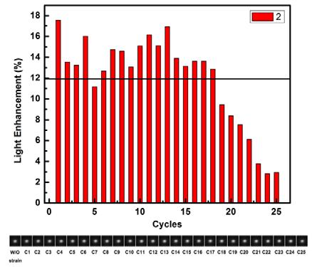
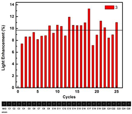
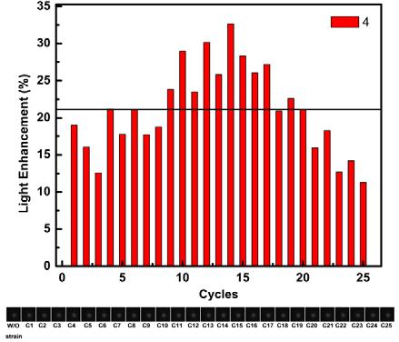
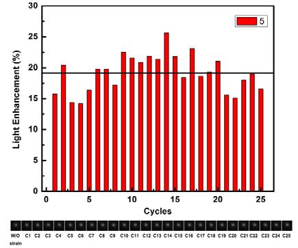
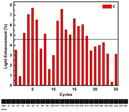
16 E: Repeatability test and reversible experiments E1: 25 repetitive on-off cycles of applying pressure on 10 far-separated NW LEDs The stability and reproducibility of the NW LED sensor array is studied by examined light emitting intensity of individual-pixels when they are under a % strain for 25 repetitive on-off cycles of applying pressure. To exclude the crosstalk from the adjacent pixels, a device consisting of sparsely distributed NW LEDs, which are numbered as 1-10, is used in this study (Fig. S13a). The average enhancement factors of these ten nano-led devices are about 15-20% under % strain (see table S1). The average fluctuation of the E factor of these 10 nano-leds is less than ±7%, much smaller than the signal level presented in Fig. 3e. Further, for the pixels we have studied, the change in E factor shows no specific trend or synchronized pattern when the device is repeatedly compressed (Fig. S13b and Fig. S14), indicating that the observed enhancement in light emission is dominated by the effect from piezoelectric charges at the ends of the NWs, rather than a change in contact-area at the ZnO-GaN junction/interface, because a change in contact area would result in a synchronized change of the E factors for all of the NW LEDs during cycled mechanical straining. 16 NATURE PHOTONICS
17 SUPPLEMENTARY INFORMATION Figure S13 Repetitive on-off cycles of applying pressure on 10 far-separated NW LEDs. a, Electroluminescence images of 10 ZnO NW LEDs, which are marked as 1 to 10. b, The enhancement E factor of these 10 nano-leds when they were repeatedly strained to % strain for 25 on-off cycles, showing a good reproducibility in the LED intensity. Detailed data of the E factor is listed in the following Table S1 and Fig. S14. Table S1. The enhancement factors of the 10 nano-leds under a strain of % in the 25 cycles. Samples Cycles #1 #2 #3 #4 #5 #6 #7 #8 #9 # Average Enhancement (%) NATURE PHOTONICS 17

18 18 NATURE PHOTONICS


19 SUPPLEMENTARY INFORMATION Figure S14 The enhancement E factors of these 10 nano-leds when they were repeatedly strained to % for 25 on-off cycles. The nano-led numbered 8 is the one shown in Fig. 3f. NATURE PHOTONICS 19

20 E2: repetitive on-off cycles of applying pressure on NW LEDs arrays, consisting of over 20,000 NW LED pixels. We add more solid data in the revised version, which proves that our devices have excellent stability, repeatability and reversibility. First, we carried out repetitive on-off cycles of applying pressure on NW LEDs arrays (Fig. S15). The images unambiguously show that the enhancement in LED intensity occurred apparently at the pixels that were being compressed by the molded pattern, and decreased when the strain was released. The images obviously show that our device has a very good repeatability and stability. It is a great step forward, since there are great challenges when extension devices from single wire to a practical array. Figure S15 Repetitive on-off cycles of applying pressure on NW LED arrays, consisting of over 20,000 NW LED pixels, showing the repeatability of the nanowire LEDs. The applied voltage was 5 V. a, An optical image of a sensor array with a nano SU-8 convex mold on the top. b-e, Electroluminescence images of the sensor array under 2 cycles of applied strain, without strain (b), strain applied (c), strain released (d) and strain reapplied (e), respectively. The images obviously show that our device has a very good repeatability and stability. 20 NATURE PHOTONICS

21 SUPPLEMENTARY INFORMATION E3: Reversible experiments by applying strain step by step We carried out a reversible experiment by applying the strain step by step, and then releasing the strain step by step. It is obviously that the light emission intensity increases when the applied strain increases step by step (step 1 to 7 of Fig. S16b), and then decreases when the applied strain releases step by step (step 8 to 14 of Fig. S16c). It shows that our devices have very good reversibility. Figure S16 Reversible experiments by applying strain step by step. The applied voltage was 5 V. a, An optical image of a sensor array with a GT logo SU-8 convex mold on the top. b-c, Electroluminescence images of the sensor array under different strains. The strain was applied on the device step by step (1-7) and then released step by step (8-14). The images obviously show that the enhancement in LED intensity occurred apparently when the applied compressive strain increases, and the enhancement of the LED intensity decreases when the applied strain releases. It shows that our devices have very good reversibility. NATURE PHOTONICS 21

22 F: More High-spatial resolution pressure images supporting Figure 4 Figure S17 Another High-spatial resolution pressure imaging of the nano-led sensor array. The applied voltage was 5 V. a, An optical image of a sensor array with a GT logo SU-8 convex mold on the top. b-c, Electroluminescence images of the sensor array without and with strain, respectively. The images obviously show that the change in LED intensity occurred apparently at the pixels that were compressed by the molded pattern, while those off the molded pattern showed almost no change in LED intensity. d, A 2-D contour map of the enhancement factor E(x,y) derived from the LED intensity images shown in (b) and (c). It directly presents the logo of Georgia Tech GT, as fabricated on the mold at the first place. G. Novel designs for the feasibility to extend the current approach to soft substrates. There are many potential applications of our strain sensor arrays, such as imaging surfaces, touch pad technology, finger print and imaging, as well as electronic skin, which is the motivation of this work. Although the current study is based on a hard substrate, it is feasible to extend the current approach to soft substrates by several means. Here we just show two of them as examples. 22 NATURE PHOTONICS

23 SUPPLEMENTARY INFORMATION First, with the same device design in the current study, just cut it into small pieces with a size about 500 μm by 500 μm, then transfer these pieces onto a soft substrates and pattern them with a μm gap between each, as shown in Figure S18a. By doing so, such device is flexible as shown in Figure S18b and S18c. Figure S18 a, b, A new design to show the feasibility to extend the current approach to soft substrates. An enlarged picture of a unit device is presented at the right side. c, An optical photo of LEDs array on a PET film showing a good flexibility of such design. Second, we can also extend current device to other materials, such as ZnO p-n homojunctions. As reported, ZnO NWs can be fabricated on any substrate, including flexible polymers and fibers, fibers and even clothes. In our recent research work, p-type Sb-doping ZnO NWs have been successfully fabricated with hydrothermal method following Dr. Voyles, PM s work (Nano Lett. 12, 1331) 2. These p-zno NWs are very stable, and they are still p-type even after 6 months. As designed in Figure S19, such p-zno/n- ZnO NWs homojunctions are used for the LEDs array. In such a design, it eliminates the hard GaN and sapphire substrate, and the flexible substrate of the device will greatly broaden the applications of our device. NATURE PHOTONICS 23

24 Figure S19 A novel design shows the feasibility to extend the current approach to soft substrates. The key tech is to use ZnO p-n homojunctions for the LED. a, A schematic of the design. b, c, 3D images demonstrate the flexibility of the device. Reference: S1. Yang, Q., Wang, W. H., Xu, S. & Wang, Z. L. Enhancing light emission of ZnO microwire-based diodes by piezo-phototronic effect. Nano Lett. 11, (2011). S2. Xia, T. H., Zhang, A. P., Gu, B. B. & Zhu, J. J. Fiber-optic refractive-index sensors based on transmissive and reflective thin-core fiber modal interferometers. Optics Communications 283, (2010). 24 NATURE PHOTONICS
Strain-Gated Field Effect Transistor of a MoS 2 -ZnO 2D-1D Hybrid-Structure
 Supporting Information Strain-Gated Field Effect Transistor of a MoS 2 -ZnO 2D-1D Hybrid-Structure Libo Chen 1, Fei Xue 1, Xiaohui Li 1, Xin Huang 1, Longfei Wang 1, Jinzong Kou 1, and Zhong Lin Wang 1,2*
Zoltán Szabó. Synthesis and characterisation of zinc-oxide thin films and nanostructures for optoelectronical purposes
 PHD theses Synthesis and characterisation of zinc-oxide thin films and nanostructures for optoelectronical purposes Zoltán Szabó Supervison: Dr. János Volk Consultant: Dr. György Hárs HAS Centre for Energy
GaN/ZnO and AlGaN/ZnO heterostructure LEDs: growth, fabrication, optical and electrical characterization
 Mater. Res. Soc. Symp. Proc. Vol. 1201 2010 Materials Research Society 1201-H01-08 GaN/ZnO and AlGaN/ZnO heterostructure LEDs: growth, fabrication, optical and electrical characterization J. Benz1, S.
Supporting Information
 Supporting Information S1. Experimental Section Growth of ZnO NW film on carbon fibers. Carbon fibers are used not only as the flexible soft substrate onto which a ZnO thin film is grown at high temperature
Ultrathin Piezotronic Transistors with 2-Nanometer Channel Lengths
 Ultrathin Piezotronic Transistors with 2-Nanometer Channel Lengths Longfei Wang,,,@ Shuhai Liu,,@ Guoyun Gao,, Yaokun Pang,, Xin Yin, & Xiaolong Feng, # Laipan Zhu,, Yu Bai,, Libo Chen,, Tianxiao Xiao,,
Engineering of efficiency limiting free carriers and interfacial energy. barrier for an enhancing piezoelectric generation
 SUPPLEMENTARY INFORMATION Engineering of efficiency limiting free carriers and interfacial energy barrier for an enhancing piezoelectric generation Jung Inn Sohn, ad SeungNam Cha, * ad Byong Gwon Song,
ZnO nanostructures epitaxially grown on ZnO seeded Si (100) substrates by chemical vapor deposition
 substrates by chemical vapor deposition") ZnO nanostructures epitaxially grown on ZnO seeded Si (100) substrates by chemical vapor deposition Zhuo Chen 1, T. Salagaj 2, C. Jensen 2, K. Strobl 2, Mim Nakarmi 1, and Kai Shum 1, a 1 Physics Department,
ZnO nanostructures epitaxially grown on ZnO seeded Si (100) substrates by chemical vapor deposition Zhuo Chen 1, T. Salagaj 2, C. Jensen 2, K. Strobl 2, Mim Nakarmi 1, and Kai Shum 1, a 1 Physics Department,
Supplementary Figure 1. Sample preparation schematic. First (Stage I), square islands of MoO 3 are prepared by either photolithography followed by
, square islands of MoO 3 are prepared by either photolithography followed by") Supplementary Figure 1. Sample preparation schematic. First (Stage I), square islands of MoO 3 are prepared by either photolithography followed by thermal evaporation and liftoff or by a process where
Supplementary Figure 1. Sample preparation schematic. First (Stage I), square islands of MoO 3 are prepared by either photolithography followed by thermal evaporation and liftoff or by a process where
A low magnification SEM image of the fabricated 2 2 ZnO based triode array is
 Chapter 6 Characteristics of Field Emission Triode 6.1 Planar Gated Field Emission Triode 6.1.1 Structural and Electrical Analysis A low magnification SEM image of the fabricated 2 2 ZnO based triode array
Hydrogen-Sensing Characteristics of Palladium-Doped Zinc-Oxide Nanostructures
 Hydrogen-Sensing Characteristics of Palladium-Doped Zinc-Oxide Nanostructures Undergraduate Researcher Saranya Sathananthan University of Tennessee, Knoxville Faculty Mentor Vinayak P. Dravid Department
Structural Properties of ZnO Nanowires Grown by Chemical Vapor Deposition on GaN/sapphire (0001)
") Structural Properties of ZnO Nanowires Grown by Chemical Vapor Deposition on GaN/sapphire (0001) F. C. Tsao 1, P. J. Huang 1, J. Y. Chen 2, C. J. Pan 3, C. J. Tun 4, C. H. Kuo 2, B. J. Pong 5, T. H. Hsueh
Structural Properties of ZnO Nanowires Grown by Chemical Vapor Deposition on GaN/sapphire (0001) F. C. Tsao 1, P. J. Huang 1, J. Y. Chen 2, C. J. Pan 3, C. J. Tun 4, C. H. Kuo 2, B. J. Pong 5, T. H. Hsueh
Outline of the talk. FIB fabrication of ZnO nanodevices. Properties of ZnO 4/19/2011. Crystal structure of ZnO. Collaborators. Wurtzite structure
 FIB fabrication of ZnO nanodevices Crystal structure of ZnO Wurtzite structure Lee Chow Department of Physics University of Central Florida 1 4 Collaborators X-ray diffraction pattern of ZnO nanorods Synthesis,
Nanostructured ZnO as a solution-processable transparent electrode material for low-cost photovoltaics
 Nanostructured ZnO as a solution-processable transparent electrode material for low-cost photovoltaics Investigators P.I: Alberto Salleo, Assistant Professor, Materials Science and Engineering Dr. Ludwig
Preparation of ZnO Nanowire Arrays Growth on Sol-Gel ZnO-Seed-Coated Substrates and Studying Its Structure and Optical Properties
 Advances in Nanomaterials 2017; 1(1): 1-5 http://www.sciencepublishinggroup.com/j/an doi: 10.11648/j.an.20170101.11 Preparation of ZnO Nanowire Arrays Growth on Sol-Gel ZnO-Seed-Coated Substrates and Studying
Path to High-Quality Films on Continuous Substrates
 Spatial Atomic Layer Deposition: A Path to High-Quality Films on Continuous Substrates t David H. Levy, Roger S. Kerr, Shelby F. Nelson, Lee W. Tutt, and Mitchell Burberry Eastman Kodak Company Rochester,
Fabrication of ZnO nanotubes using AAO template and sol-gel method
 Journal of Optoelectronic and Biomedical Materials Volume 1, Issue 1, March 2009, p. 15-19 Fabrication of ZnO nanotubes using AAO template and sol-gel method S. Öztürk a, N. Taşaltin a, n. Kilinç a, Z.
Piezotronic Effect on the Sensitivity and Signal Level of Schottky Contacted Proactive Micro/Nanowire Nanosensors
 Piezotronic Effect on the Sensitivity and Signal Level of Schottky Contacted Proactive Micro/Nanowire Nanosensors Caofeng Pan,,, Ruomeng Yu,, Simiao Niu, Guang Zhu, and Zhong Lin Wang,, * ARTICLE School
A Hybrid Piezoelectric Structure for Wearable Nanogenerators
 www.materialsviews.com A Hybrid Piezoelectric Structure for Wearable Nanogenerators Minbaek Lee, Chih-Yen Chen, Sihong Wang, Seung Nam Cha, Yong Jun Park, Jong Min Kim, Li-Jen Chou, and Zhong Lin Wang*
Large-Scale Synthesis of Six-Nanometer-Wide ZnO Nanobelts
 J. Phys. Chem. B 2004, 108, 8773-8777 8773 Large-Scale Synthesis of Six-Nanometer-Wide ZnO Nanobelts Xudong Wang, Yong Ding, Christopher J. Summers, and Zhong Lin Wang* School of Materials Science and
Reagent-Free Electrophoretic Synthesis of Few-Atom- Thick Metal Oxide Nanosheets
 Supporting Information Reagent-Free Electrophoretic Synthesis of Few-Atom- Thick Metal Oxide Nanosheets Chengyi Hou,*,, Minwei Zhang, Lili Zhang, Yingying Tang, Hongzhi Wang, and Qijin Chi*, State Key
LIQUID JUNCTION PHOTOCELLS SYNTHESIZED WITH DYE COATED ZINC OXIDE FILMS. Department of Physics, University of Peradeniya, Peradeniya, Sri Lanka
 J Sci.Univ.Kelaniya 5 (2010) : 25-31 LIQUID JUNCTION PHOTOCELLS SYNTHESIZED WITH DYE COATED ZINC OXIDE FILMS P. SAMARASEKARA Department of Physics, University of Peradeniya, Peradeniya, Sri Lanka Email:
Supporting Information
 Supporting Information An efficient broadband and omnidirectional light-harvesting scheme employing the hierarchical structure based on ZnO nanorod/si 3 N 4 -coated Si microgroove on 5-inch single crystalline
The electrical properties of ZnO MSM Photodetector with Pt Contact Electrodes on PPC Plastic
 Journal of Electron Devices, Vol. 7, 21, pp. 225-229 JED [ISSN: 1682-3427 ] Journal of Electron Devices www.jeldev.org The electrical properties of ZnO MSM Photodetector with Pt Contact Electrodes on PPC
Les LEDs à Base de l Oxyde de Zinc D. Rogers : Nanovation & Universite de Technologie de Troyes F. Hosseini Teherani : Nanovation, France
 Les LEDs à Base de l Oxyde de Zinc D. Rogers : Nanovation & Universite de Technologie de Troyes F. Hosseini Teherani : Nanovation, France OUTLINE 1. Problems with Todays LEDs 2. ZnO vs GaN 3. Nanovation
A High-Reliability Kevlar Fiber-ZnO Nanowires Hybrid Nanogenerator and its Application on Self-Powered UV Detection
 A High-Reliability Kevlar Fiber-ZnO Nanowires Hybrid Nanogenerator and its Application on Self-Powered UV Detection Lu Zhang, Suo Bai, Chen Su, Youbin Zheng, Yong Qin, * Chen Xu, * and Zhong Lin Wang *
Supplementary Figure 1. EL spectral characteristics. (a)
") Supplementary Figure 1. EL spectral characteristics. (a) Angular dependence of normalized light intensity at 540 nm according to ZnO layers; Lambertian emission pattern (black square), ZnO-F (red circle),
Supplementary Figure 1. EL spectral characteristics. (a) Angular dependence of normalized light intensity at 540 nm according to ZnO layers; Lambertian emission pattern (black square), ZnO-F (red circle),
Piezoelectric Nanogenerator Using p-type ZnO Nanowire Arrays
 Letter Subscriber access provided by Georgia Tech Library Piezoelectric Nanogenerator Using p-type ZnO Nanowire Arrays Ming-Pei Lu, Jinhui Song, Ming-Yen Lu, Min-Teng Chen, Yifan Gao, Lih-Juann Chen, and
Center for Nanoscience and Nanotechnology, School of Materials Science and Engineering, Georgia Institute of Technology, Atlanta, Georgia
 Copyright 2002 by the American Chemical Society VOLUME 106, NUMBER 49, DECEMBER 12, 2002 LETTERS Self-Assembled Nanowire-Nanoribbon Junction Arrays of ZnO Puxian Gao Center for Nanoscience and Nanotechnology,
Department of Electrical & Computer Engineering, The Ohio State University, 205 Dreese Lab, 2015
 Supplemental Information for Defect Manipulation to Control ZnO Micro-/Nanowire Metal Contacts Jonathan W. Cox, Geoffrey M. Foster, Alexander Jarjour, Holger von Wenckstern, Marius Grundmann, and Leonard
ZnO Thin Films Synthesized by Chemical Vapor Deposition
 ZnO Thin Films Synthesized by Chemical Vapor Deposition Zhuo Chen *1, Kai Shum *2, T. Salagaj #3, Wei Zhang #4, and K. Strobl #5 * Physics Department, Brooklyn College of the City University of New York
Synthesis and Characterization of Mn 2+ Doped Zn 2. Phosphor Films by Combustion CVD Method
 Synthesis and Characterization of Mn 2+ Doped Zn 2 Phosphor Films by Combustion CVD Method Z. T. Kang a, Y. Liu b, B. K. Wagner a, R. Gilstrap a, M. Liu b, and C. J. Summers a a Phosphor Technology Center
Structural, Optical & Surface Morphology of Zinc Oxide (ZnO) Nanorods in Molten Solution
 Nanorods in Molten Solution") Journal of Materials Science and Engineering B 6 (3-4) (2016) 68-73 doi: 10.17265/2161-6221/2016.3-4.002 D DAVID PUBLISHING Structural, Optical & Surface Morphology of Zinc Oxide (ZnO) Nanorods in Molten
Journal of Materials Science and Engineering B 6 (3-4) (2016) 68-73 doi: 10.17265/2161-6221/2016.3-4.002 D DAVID PUBLISHING Structural, Optical & Surface Morphology of Zinc Oxide (ZnO) Nanorods in Molten
NANOSTRUCTURAL ZnO FABRICATION BY VAPOR-PHASE TRANSPORT IN AIR
 International Journal of Modern Physics B Vol. 18, No. 0 (2004) 1 8 c World Scientific Publishing Company NANOSTRUCTURAL ZnO FABRICATION BY VAPOR-PHASE TRANSPORT IN AIR C. X. XU, X. W. SUN, B. J. CHEN,
Annealing Influence on the Optical Properties of Nano ZnO
 Available online www.ejaet.com European Journal of Advances in Engineering and Technology, 2014, 1(1): 69-73 Research Article ISSN: 2394-658X Annealing Influence on the Optical Properties of Nano ZnO Saad
Study of Structural and Optical Properties of ZnO Thin Films Produced by Sol Gel Methods
 Sensors and Materials, Vol. 28, No. 5 (2016) 523 530 MYU Tokyo 523 S & M 1205 Study of Structural and Optical Properties of ZnO Thin Films Produced by Sol Gel Methods Huai-Shan Chin, Long-Sun Chao, * and
A Solution Processed ZnO Thin Film
 Applied Mechanics and Materials Vols. 239-240 (2013) pp 1585-1588 Online available since 2012/Dec/13 at www.scientific.net (2013) Trans Tech Publications, Switzerland doi:10.4028/www.scientific.net/amm.239-240.1585
Splendid One-Dimensional Nanostructures of Zinc Oxide: A New Nanomaterial Family for Nanotechnology
 Splendid One-Dimensional Nanostructures of Zinc Oxide: A New Nanomaterial Family for Nanotechnology Zhong Lin Wang* School of Materials Science and Engineering, Georgia Institute of Technology, Atlanta,
Epitaxial Growth of ZnO Nanowires on Graphene-Au
 Epitaxial Growth of ZnO Nanowires on Graphene-Au 1 Schematic of Growth Process Nanorod Nanowire Nanoribbon Giri et al.. ACS Appl. Mater. Interf. 6, 377 (2014). 2 1 FESEM image of ZnO NWs/NRBs Grown on
Supporting Information
 Supporting Information Size Tunable ZnO Nanoparticles to Enhance Electron Injection in Solution Processed QLEDs Jiangyong Pan,, Jing Chen,, Qianqian Huang, Qasim Khan, Xiang Liu, Zhi Tao, Zichen Zhang,
Influence of Texture Depth and Layer Thickness of Crater-like Textured ZnO on the Efficiency of Thin Film Solar Cell
 Influence of Texture Depth and Layer Thickness of Crater-like Textured ZnO on the Efficiency of Thin Film Solar Cell Rummana Rahman, Tamanna Motahar, and Tahsin Rahman Department of Electrical and Computer
Supplementary Information
 Electronic Supplementary Material (ESI) for ChemComm. This journal is The Royal Society of Chemistry 2015 Supplementary Information Comprehensive biosensor integrated with ZnO nanorods FETs array for selective
Characterization of Zinc Oxide Nanolaminate Films. B. J. Oleson, L. M. Bilke, J. S. Krueger, S. T. King
 Introduction Characterization of Zinc Oxide Nanolaminate Films B. J. Oleson, L. M. Bilke, J. S. Krueger, S. T. King Department of Physics, University of Wisconsin La Crosse Abstract: This project sought
Supplementary Fig. 1 Atomic force microscopy topography images Two-dimensional atomic force microscopy images (with an area of 1 m 1 m) of Cu and
 of Cu and") Supplementary Fig. 1 Atomic force microscopy topography images Two-dimensional atomic force microscopy images (with an area of 1 m 1 m) of Cu and Cu(O = 5.0%) films deposited on 20-nm-thick ZnO films during
Supplementary Fig. 1 Atomic force microscopy topography images Two-dimensional atomic force microscopy images (with an area of 1 m 1 m) of Cu and Cu(O = 5.0%) films deposited on 20-nm-thick ZnO films during
Piezoelectric Potential Output from ZnO Nanowire Functionalized with p-type Oligomer
 Piezoelectric Potential Output from ZnO Nanowire Functionalized with p-type Oligomer NANO LETTERS 2008 Vol. 8, No. 1 203-207 Jinhui Song, Xudong Wang, Jin Liu, Huibiao Liu,, Yuliang Li, and Zhong Lin Wang*,
Shape Memory Alloy Micro-Actuator for Handling of Head Gimbal Assembly
 AIJSTPME (2011) 4(4): 1-8 Shape Memory Alloy Micro-Actuator for Handling of Head Gimbal Assembly Prapaipittayakhun K. Department of Mechanical Engineering, Faculty of Engineering, Chulalongkorn University,
Electronic Supplementary Information
 Electronic Supplementary Material (ESI) for Journal of Materials Chemistry A. This journal is The Royal Society of Chemistry 2014 Electronic Supplementary Information Photogenerated Electron Reservoir
SPONTANEOUS AND STIMULATED EMISSION OF ZnO NANORODS OF DIFFERENT SHAPE
 SPONTANEOUS AND STIMULATED EMISSION OF ZnO NANORODS OF DIFFERENT SHAPE A.N. Gruzintsev, A.N. Redkin,**G.A. Emelchenko, *C. Barthou Institute of Microelectronics Technology, Russian Academy of Sciences,
Supporting information
 Supporting information Blue Quantum Dot Light-Emitting Diodes with High Electroluminescent Efficiency Lishuang Wang,, Jie Lin *, Yongsheng Hu, Xiaoyang Guo,Ying Lv, Zhaobing Tang,, Jialong Zhao *, Yi Fan,
Piezotronic Effect on the Output Voltage of P3HT/ZnO Micro/ Nanowire Heterojunction Solar Cells
 pubs.acs.org/nanolett Piezotronic Effect on the Output Voltage of P3HT/ZnO Micro/ Nanowire Heterojunction Solar Cells Ya Yang, Wenxi Guo, Yan Zhang, Yong Ding, Xue Wang, and Zhong Lin Wang* School of Material
Optical Properties of Aligned Zinc Oxide Nanorods
 Optical Properties of Aligned Zinc Oxide Nanorods For use in Extremely Thin Absorber Solar Cells Kieren Bradley Prof. Dave Cherns, Dr. David Fermin, Dr. Martin Cryan 1 Project Aims To be able to grow zinc
A Facile Method for Enhancing the Sensing Performance of Zinc Oxide. Nanofibers Gas Sensors
 Electronic Supplementary Information (ESI): A Facile Method for Enhancing the Sensing Performance of Zinc Oxide Nanofibers Gas Sensors Pei-Pei Wang a, Qi Qi a, Rui-Fei Xuan a,b, Jun Zhao a, Li-Jing Zhou
Optimizing and Improving the Growth Quality of ZnO Nanowire Arrays Guided by Statistical Design of Experiments
 Optimizing and Improving the Growth Quality of ZnO Nanowire Arrays Guided by Statistical Design of Experiments Sheng Xu, Nagesh Adiga, Shan Ba, Tirthankar Dasgupta, C. F. Jeff Wu,, * and Zhong Lin Wang,
Keywords: Thin films, Zinc Oxide, Sol-gel, XRD, Optical properties
 Advanced Materials Research Vol. 895 (2014) pp 250-253 Online available since 2014/Feb/13 at www.scientific.net (2014) Trans Tech Publications, Switzerland doi:10.4028/www.scientific.net/amr.895.250 Structural
Roll-to-roll fabrication of large scale and regular arrays of three-dimensional nanospikes
 Roll-to-roll fabrication of large scale and regular arrays of three-dimensional nanospikes for high efficiency and flexible photovoltaics Siu-Fung Leung, 1 Leilei Gu, 1,+ Qianpeng Zhang, 1,+ Kwong-Hoi
Technology and TEM characterization of Al doped ZnO nanomaterials
 Technology and TEM characterization of Al doped ZnO nanomaterials 國立成功大學 (NCKU) 材料科學及工程系 (MSE) 劉全璞 (Chuan-Pu Liu) Outline Introduction of ZnO Doping ZnO nanomaterials in CVD Al doped ZnO Nanowires Al doped
ANTIMONY DOPED P-TYPE ZINC OXIDE FOR PIEZOTRONICS AND OPTOELECTRONICS
 ANTIMONY DOPED P-TYPE ZINC OXIDE FOR PIEZOTRONICS AND OPTOELECTRONICS A Dissertation Presented to The Academic Faculty By Ken C. Pradel In Partial Fulfillment Of the Requirements for the Degree Doctor
Renewable energy plays a crucial role
 Anisotropic Outputs of a Nanogenerator from Oblique-Aligned ZnO Nanowire Arrays Cheng-Ying Chen,, Jun-Han Huang,,, Jinhui Song, Yusheng Zhou, Long Lin, Po-Chien Huang, Yan Zhang,,^ Chuan-Pu Liu,,, Jr-Hau
Growth of ZnO nanotube arrays and nanotube based piezoelectric nanogenerators
 PAPER www.rsc.org/materials Journal of Materials Chemistry Growth of ZnO nanotube arrays and nanotube based piezoelectric nanogenerators Yi Xi, ab Jinhui Song, a Sheng Xu, a Rusen Yang, a Zhiyuan Gao,
Solution-processed ZnO films as an alternative to sputtered buffer layers for inorganic photovoltaics
 Solution-processed ZnO films as an alternative to sputtered buffer layers for inorganic photovoltaics ICONN 214, Adelaide Dr. Enrico Della Gaspera CSIRO MATERIALS SCIENCE AND ENGINEERING / FUTURE MANUFACTURING
Room-temperature larger-scale highly ordered nanorod imprints of ZnO film
 Room-temperature larger-scale highly ordered nanorod imprints of ZnO film Zabu Kyaw, 1 Wang Jianxiong, 1 Kapil Dev, 1 Swee Tiam Tan, 1,2 Zhengang Ju, 1 Zi-Hui Zhang, 1 Yun Ji, 1 Namig Hasanov, 1 Wei Liu,
Alumina stabilized ZnO-graphene anode for lithium ion
 Electronic Supplementary Material (ESI) for Nanoscale. This journal is The Royal Society of Chemistry 2014 Supporting Information for Alumina stabilized ZnO-graphene anode for lithium ion batteries via
Large Work Function Modulation of Monolayer MoS 2. by Ambient Gases
 Supporting Information Large Work Function Modulation of Monolayer MoS 2 by Ambient Gases Si Young Lee, 1 Un Jeong Kim, 3,, * JaeGwan Chung, 4 Honggi Nam, 1,2 Hye Yun Jeong, 1,2 Gang Hee Han, 1 Hyun Kim,
The structural and optical properties of ZnO thin films prepared at different RF sputtering power
 Journal of King Saud University Science (2013) 25, 209 215 King Saud University Journal of King Saud University Science www.ksu.edu.sa www.sciencedirect.com ORIGINAL ARTICLE The structural and optical
Dye Sensitized Solar Cells (DSSC) Performance Reviewed from the Composition of Titanium Dioxide (TiO2)/Zinc Oxide (ZnO)
 Performance Reviewed from the Composition of Titanium Dioxide (TiO2)/Zinc Oxide (ZnO)") IOP Conference Series: Materials Science and Engineering PAPER OPEN ACCESS Dye Sensitized Solar Cells (DSSC) Performance Reviewed from the Composition of Titanium Dioxide (TiO2)/Zinc Oxide (ZnO) To cite
IOP Conference Series: Materials Science and Engineering PAPER OPEN ACCESS Dye Sensitized Solar Cells (DSSC) Performance Reviewed from the Composition of Titanium Dioxide (TiO2)/Zinc Oxide (ZnO) To cite
Replacing a Battery by a Nanogenerator with 20 V Output
 Replacing a Battery by a Nanogenerator with 2 V Output Youfan Hu, Long Lin, Yan Zhang, and Zhong Lin Wang * We have been working on self-powered nanotechnology since 2 with the aim to build self-powered
THE DEVELOPMENT AND MANUFACTURE OF FIXED- ULTRASONIC INSPECTION REFERENCE REFLECTORS AND TRANSDUCERS FOR COMPRESSOR BLADE DOVETAILS
 International Workshop SMART MATERIALS, STRUCTURES & NDT in AEROSPACE Conference NDT in Canada 2011 2-4 November 2011, Montreal, Quebec, Canada THE DEVELOPMENT AND MANUFACTURE OF FIXED- ULTRASONIC INSPECTION
MOF-Derived Zn-Mn Mixed Hollow Disks. with Robust Hierarchical Structure for High-Performance. Lithium-Ion Batteries
 Electronic Supplementary Material (ESI) for Journal of Materials Chemistry A. This journal is The Royal Society of Chemistry 2017 Electronic Supplementary Information (ESI) MOF-Derived Zn-Mn Mixed Oxides@Carbon
Influence of Growth Time on Zinc Oxide Nano Rods Prepared By Dip Coating Method
 Influence of Growth Time on Zinc Oxide Nano Rods Prepared By Dip Coating Method P.Thamarai selvan 1, M.Venkatachalam 2, M.Saroja 2, P.Gowthaman 2, S.Ravikumar 3, S.Shankar 2 Department of Electronics &
Investigation of Structure, Morphology, Optical And Luminescent Properties of Hydrothermally Grown Zno Nanorods for Photocatalytic Applications
 Investigation of Structure, Morphology, Optical And Luminescent Properties of Hydrothermally Grown Zno Nanorods for Photocatalytic Applications S.Kumar 1, J.Deenathayalan 2, M.Baskaran 3, D.D.Saravanan
Journal of Crystal Growth
 Journal of Crystal Growth 319 (2011) 39 43 Contents lists available at ScienceDirect Journal of Crystal Growth journal homepage: www.elsevier.com/locate/jcrysgro Epitaxial growth of Cu 2 O and ZnO/Cu 2
Low-temperature growth and Raman scattering study of. vertically aligned ZnO nanowires on Si substrate
 Low-temperature growth and Raman scattering study of vertically aligned ZnO nanowires on Si substrate Ye Zhang, Hongbo Jia, Dapeng Yu a), Rongming Wang, Xuhui Luo School of Physics, National Key Laboratory
PZT/ZnO EXPERIMENT MODELLING
 Mat. Res. Soc. Symp. Proc. Vol. 655 2001 Materials Research Society High Frequency Thin Film Acoustic Ferroelectric Resonators Paul Kirby a, Qing-Xin Su a, Eiju Komuro b, Masaaki Imura b, Qi Zhang, and
Structural and Optical Properties of ZnO Nanostructured Layers Deposited by Electrochemical Method on Conductive Multi-Crystalline Si Substrates
 Bulg. J. Phys. 40 (2013) 229 236 Structural and Optical Properties of ZnO Nanostructured Layers Deposited by Electrochemical Method on Conductive Multi-Crystalline Si Substrates M. Petrov 1, K. Lovchinov
ABSTRACT. GROWTH AND TRANSPORT PROPERTIES OF Sb-DOPED ZnO NANO/MICROWIRES. by Nada Ali Masmali
 ABSTRACT GROWTH AND TRANSPORT PROPERTIES OF Sb-DOPED ZnO NANO/MICROWIRES by Nada Ali Masmali In this research, the transport properties of Sb-doped ZnO wires were investigated. ZnO:Sb wires were grown
GCEP award #40654: High-Efficiency, Low-Cost Thin Film Solar Cells
 GCEP award #40654: High-Efficiency, Low-Cost Thin Film Solar Cells Alberto Salleo, Dept. of Materials Science and Engineering, Stanford University Yi Cui, Dept. of Materials Science and Engineering, Stanford
GaN Growth on Si Using ZnO Buffer Layer. layer thickness on GaN quality was found to be important.
 Mat. Res. Soc. Symp. Proc. Vol. 764 2003 Materials Research Society C7.7.1 GaN Growth on Si Using ZnO Buffer Layer K.C. Kim, S.W. Kang, O. Kryliouk and T.J. Anderson Department of Chemical Engineering,
ZnO Thin Films Generated by Ex-Situ Thermal Oxidation of Metallic Zn for Photovoltaic Applications
 Macalester Journal of Physics and Astronomy Volume 4 Issue 1 Spring 2016 Article 12 May 2016 ZnO Thin Films Generated by Ex-Situ Thermal Oxidation of Metallic Zn for Photovoltaic Applications Kovas Zygas
Mechanical Simulation of Probing on SMART POWER POA devices
 Luca Cecchetto STMicroelectronics Mechanical Simulation of Probing on SMART POWER POA devices June 8 to 11, 2008 San Diego, CA USA Authors L. Cecchetto, L. Zullino, R. Vallauri, L. Cerati, A. Andreini
Chemical Engineering, Xiamen University, Xiamen ,China. 4
 Supporting Information for : One-pot synthesis of superfine core-shell Cu@metal nanowires for highly tenacious transparent LED dimmer Huachun Wang 1, Chenping Wu 1, Youyang Huang 1, Feipeng Sun 1, Na Lin
Method to Convert a Horizontal Furnace to Grow ZnO Nanowires for Gas Sensing by the VLS Method.
 Method to Convert a Horizontal Furnace to Grow ZnO Nanowires for Gas Sensing by the VLS Method. Sushma Nandhyala, Michael Haji-Sheikh, Martin Kocanda, and Suma Rajashankar Electrical Engineering Department,
Infrastructure for Rapid Assessment of Reliability
 Infrastructure for Rapid Assessment of Reliability Infrastructure and process improvements in the reliability testing of a high density microelectronic packaging technology Hannah Varner Draper Outline
Supporting Information. Observing Solid-state Formation of Oriented Porous. Functional Oxide Nanowire Heterostructures by in situ
 Supporting Information Observing Solid-state Formation of Oriented Porous Functional Oxide Nanowire Heterostructures by in situ TEM Jo-Hsuan Ho,+, Yi-Hsin Ting,,+, Jui-Yuan Chen,+, Chun-Wei Huang, Tsung-Chun
Supporting Information
 This journal is The Royal Society of Chemistry 011 Supporting Information Vertically-Aligned ZnO Nanorods Doped with Lithium for Polymer Solar Cells: Defect Related Photovoltaic Properties Pipat Ruankham,
THE EFFECTS OF DOPING CONCENTRATION ON THE ELECTRICAL PERFORMANCE OF DC-SPUTTERED p-zno/n-si HETEROJUNCTION
 THE EFFECTS OF DOPING CONCENTRATION ON THE ELECTRICAL PERFORMANCE OF DC-SPUTTERED p-zno/n-si HETEROJUNCTION Dao Anh Tuan, Bui Khac Hoang, Nguyen Van Hieu, Le Vu Tuan Hung Department of Applied Physics,
Simulation study of optical transmission properties of ZnO thin film deposited on different substrates
 American Journal of Optics and Photonics 2013; 1(1) : 1-5 Published online February 20, 2013 (http://www.sciencepublishinggroup.com/j/ajop) doi: 10.11648/j.ajop.20130101.11 Simulation study of optical
CHAPTER 8 SUMMARY AND FUTURE SCOPE
 CHAPTER 8 SUMMARY AND FUTURE SCOPE The potential of room temperature ferromagnetism in many diluted magnetic semiconductors has opened up a new route for realization of spintronic devices. Based on the
Etching of ZnO towards the Development of ZnO Homostructure LEDs
 Invited Paper Etching of ZnO towards the Development of ZnO Homostructure LEDs Kathryn Minder a, Ferechteh Hosseini Teherani b, Dave Rogers b,c, Can Bayram a, Ryan McClintock a, Patrick Kung a, and Manijeh
Valve-Based Microfluidic Compression Platform: Single Axon Injury and Regrowth
 Supplementary Material (ESI) for Lab on a Chip This Journal is The Royal Society of Chemistry 2011 Valve-Based Microfluidic Compression Platform: Single Axon Injury and Regrowth Suneil Hosmane a, Adam
Electric field induced reversible control of visible. photoluminescence from ZnO nanoparticles
 Electric field induced reversible control of visible photoluminescence from ZnO nanoparticles Manoranjan Ghosh,# and A. K. Raychaudhuri $ DST Unit for Nanoscience, S. N. Bose National Centre for Basic
Chapter VI Development of ISFET model. simulation
 Chapter VI Development of ISFET model using ZnO as gate and its simulation Introduction Theory of ISFET Experimental work Results and discussion Conclusion 6.1 General: The human bodies ph and electrolyte
Abstract. Keywords: Zinc Oxide, Eu doped ZnO, Dy doped ZnO, Thin film INTERNATIONAL JOURNAL OF INFORMATION AND COMPUTING SCIENCE ISSN NO:
 Synthesis and Structural study of Rare Earth activated ZnO Thin film Pawan Kumar Department of Physics, University Institute of Sciences, Chandigarh University, Gharuan (Mohali), Punjab (India) e-mail-pawan.uis@cumail.in
Theerapong Santhaveesuk, * Duangmanee Wongratanaphisan and Supab Choopun
 NU Science Journal 2009; 6(S1): 43-50 Ethanol Sensing Property of Tetrapods Prepared by Thermal Oxidation of Zn and TiO 2 Mixture Theerapong Santhaveesuk, * Duangmanee Wongratanaphisan and Supab Choopun
ZnO mixes it up with nitride semiconductors
 98 Technology focus: Wide-bandgap materials ZnO mixes it up with nitride semiconductors Mike Cooke reports on recent research that combines ZnO with nitride semiconductors for transparent conduction, light
A hybrid concept as a new approach for the micro-production of magnetic actuators
 1 A hybrid concept as a new approach for the micro-production of magnetic actuators Rissing, L. H. H.; Creutzburg, T.; Steffens, M.; Reuter, G.; Lenarz, T. ABSTRACT Actuators that are widely used in industrial
Supporting Information for
 Supporting Information for Rupture of Lipid Membranes Induced by Amphiphilic Janus Nanoparticles Kwahun Lee, Liuyang Zhang, Yi Yi, Xianqiao Wang, Yan Yu* Department of Chemistry, Indiana University, Bloomington,
Transparent ALD-grown Ta2O5 protective layer for highly stable ZnO photoelectrode in solar water splitting
 Electronic Supplementary Material (ESI) for Chemical Communications. This journal is The Royal Society of Chemistry 2015 Transparent ALD-grown Ta2O5 protective layer for highly stable ZnO photoelectrode
Growth and Characterizations of Electrochemically Deposited ZnO Thin Films
 Solid State Phenomena Vols. 124-126 (2007) pp 135-138 Online available since 2007/Jun/15 at www.scientific.net (2007) Trans Tech Publications, Switzerland doi:10.4028/www.scientific.net/ssp.124-126.135
Thin-film barriers using transparent conducting oxides for organic light-emitting diodes
 Thin-film barriers using transparent conducting oxides for organic light-emitting diodes Ho Nyeon Lee Hyung Jung Kim Young Min Yoon Abstract This study covers thin-film barriers using inorganic barriers
Selective Growth of ZnO Nanorod Arrays on a GaN/Sapphire Substrate Using a Proton Beam Written Mask
 Article Subscriber access provided by NATIONAL UNIV OF SINGAPORE Selective Growth of ZnO Nanorod Arrays on a GaN/Sapphire Substrate Using a Proton Beam Written Mask H. L. Zhou, P. G. Shao, S. J. Chua,
Deposition of aluminum-doped zinc oxide films by RF magnetron sputtering and study of their surface characteristics
 Surface and Coatings Technology 174 175 (2003) 187 192 Deposition of aluminum-doped zinc oxide films by RF magnetron sputtering and study of their surface characteristics a b b a a, S.H. Jeong, S. Kho,