Electric field induced reversible control of visible. photoluminescence from ZnO nanoparticles
|
|
|
- Edward Francis
- 6 years ago
- Views:
Transcription
1 Electric field induced reversible control of visible photoluminescence from ZnO nanoparticles Manoranjan Ghosh,# and A. K. Raychaudhuri $ DST Unit for Nanoscience, S. N. Bose National Centre for Basic Sciences, Block-JD, Sector-3, Salt Lake, Kolkata , INDIA Reversible control of the photoluminescence of ZnO occurring in the visible range, has been achieved by application of a few volts (< 5V) to a device consisting of nanostructured ZnO film sandwiched between Indium Tin Oxide electrode and polyethylene oxide-lithium perchlorate, a solid polymer electrolyte. The photoluminescence intensity shows nearly 100% modulation with a response time less than 30 seconds, when the bias is applied at the electrolyte-electrode. A model is proposed for the observed effect that is based on defect states of ZnO and the band bending at the ZnO-electrolyte interface that can be changed by the applied bias. Keywords: Electrophotoluminescence, ZnO nanostructure-electrolyte, Visible emission, Band bending. Present address: Bhabha Atomic Research Centre, Mumbai , INDIA # mghosh@barc.gov.in, $ E mail: arup@bose.res.in 1
2 ZnO, a wide band gap (3.3 ev) semiconductor with wurtzite structure (P63mc) is a well-known material for applications in the ultra violet (UV) region of the electromagnetic spectrum. Over the past decade, tremendous progress in research has been achieved for the use of ZnO as an optoelectronic material. 1 In particular, nanostructured ZnO that can be fabricated at temperatures below C, can be used for innovative applications. The room temperature photoluminescence (PL) of ZnO nanoparticles (NPs) of size below 20 nm typically exhibits near band edge (NBE) emission in the UV region and a broad emission band in the visible region of the spectrum. 2 Fine control of this defect related visible PL is challenging because of its dependence on many environmental parameters. Factors like size and shape of the material, polar nature of the surrounding medium and type of defects involved in the emission processes were identified and the positively charged oxygen vacancies were commonly attributed as likely origin of this emission. 3,4 It will be an interesting proposition if a full reversible control of this visible emission is achieved by application of a voltage bias. This will not only be of scientific interest but can also have an application potential. NBE emission of a semiconductor, that has an excitonic origin, can be controlled by application of electric field at the semiconductor-metal (S-M) and semiconductorelectrolyte (S-E) junction. For example, reversible change in excitonic PL from epitaxial GaN 5 was seen by application of electric field at the S-M junction. In a recent report, reduction of the visible emission and enhancement of the UV emission has been observed in a ZnO based Metal-Insulator-Semiconductor (MIS) structure on application of a bias. 6 Reduction of PL from n-gaas electrode immersed in aqueous ditelluride 2
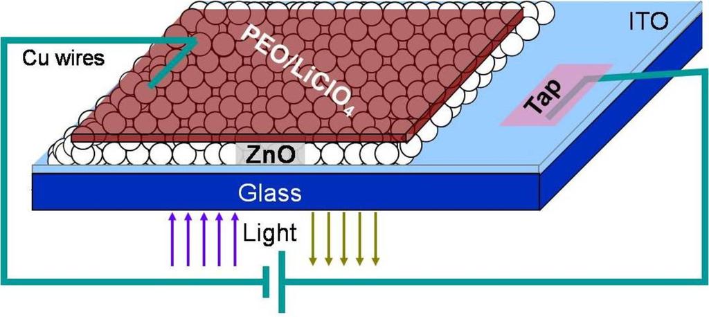
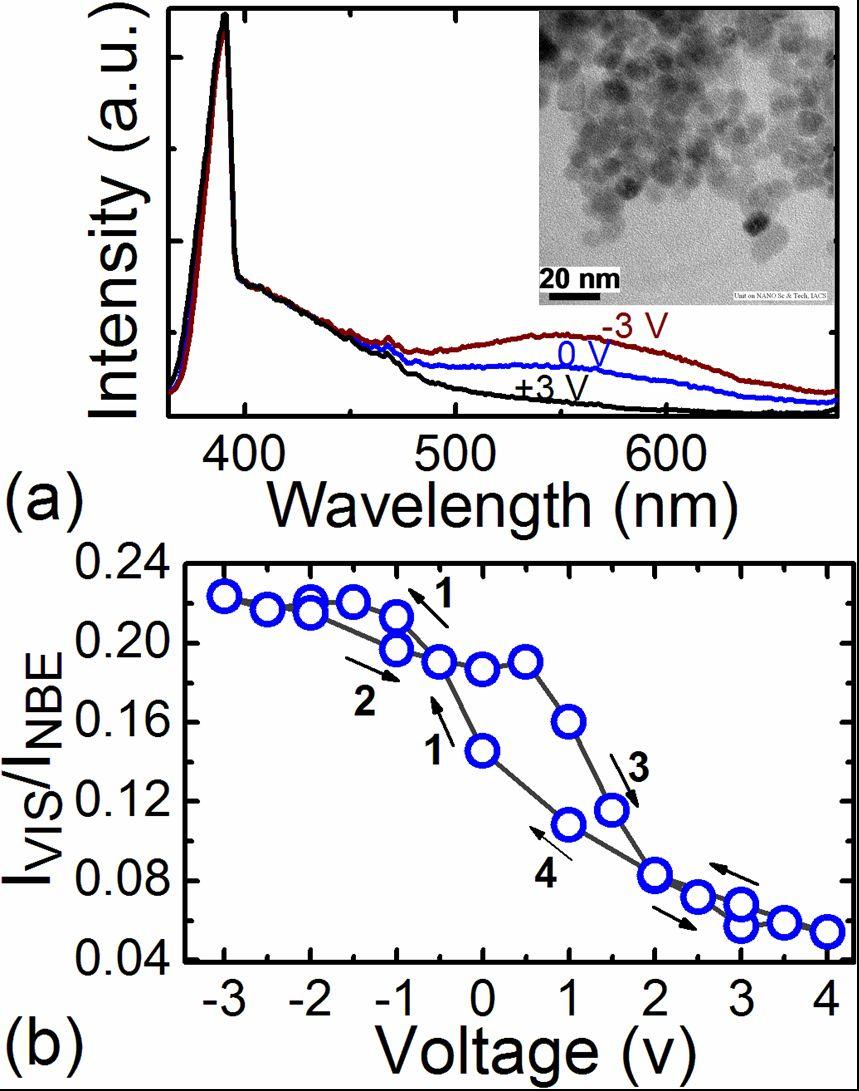
3 electrolyte by application of external voltage has also been reported. 7 Recently it has been demonstrated by us that ZnO NPs suspended in an electrolytic solution show reduced visible emission. 8 In this paper we describe reversible control (reduction as well as enhancement) of the visible PL from ZnO NPs by application of small voltage (< 5 V) at S-E junction. The observed enhancement as well as reduction is substantial. A device consisting of Indium Tin Oxide (ITO)/ZnO NPs/polymeric electrolyte (figure 1) has been constructed to demonstrate the effect field controlled visible PL. The film of ZnO NPs of size ~10 nm [see inset of Figure 2 (a)], synthesized by solution route 9 is obtained by adding NP-ethanol dispersion on ITO coated glass substrate at room temperature. To ensure the presence of a ZnO layer all over the surface, a thick film is deposited. The average thickness was found to be nm. When the ZnO film dries off, a gel of polyethylene oxide (PEO, MW ) and lithium perchlorate (LiClO 4 ) is deposited on the ZnO layer. After the gel becomes solid, it holds securely the electrical connections (Cu wires) as shown in Fig. 1. The PL spectra were measured by a Spectrofluorimeter (Jobin Yvon Fluromax 3). The bias voltages were supplied by a Stanford Research System DS345 synthesized function generator. The device has been illuminated by UV light of energy higher than the band gap of ZnO. However, the upper energy is limited by the transmittance of ITO. We excite the device through ITO glass face and the emitted signal is collected in the reflection mode. In this arrangement, the thick ZnO film acts as an absorbing layer before the illumination reaches the electrolyte at the interface. This eliminates the PL from the polymer that occurs at around 425 nm. ZnO NPs sandwiched in the device show maximum NBE PL near 390 nm and visible PL around nm when illuminated in the window
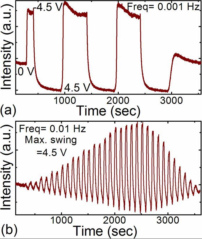
4 nm through ITO. (See supplementary material at [URL] for absorption and PL spectra of individual component). The PL spectra from the device [Fig. 2 (a)], matches with that obtained from the colloidal ZnO NPs taken in suspension. 3,8 However, the relative intensity of the surface related broad visible PL is reduced due to the surface passivation of ZnO NPs by PEO-LiClO 4 layer. A shoulder around nm superimposed on the NBE emission appears in the PL spectra due to the emission from PEO-LiClO 4 as stated before. However, this does not affect the visible PL signal near nm range. The main result of this work is the remarkable change in the visible PL from ZnO NPs by application of voltage bias. Nearly 100 percent modulation of the visible PL intensity is achieved [Fig. 2(a)] while maximum change occurs within ± 1.5 V. PL intensity increases when the device is biased as depicted in figure 1 and vice versa. In Fig 2(b), we show voltage dependence of the ratio I VIS /I NBE, where I VIS and I NBE are the intensities of visible (~550 nm) and NBE (~390 nm) emissions respectively. I VIS /I NBE continuously decreases when the bias is changed from -2 V to +2 V. The ratio can be changed by nearly a factor of 3 when the bias is cycled between ±3V and it saturates for bias beyond that. The bias cycling at a finite rate can cause a hysteresis effect in the observed values of I VIS /I NBE due to finite response time. For the data presented in Fig 2(b), the scan time for the full voltage cycle is 30 min. For longer cycling time the hysteresis becomes smaller and eventually vanishes. The finite response time seen in the device arises due to polymeric nature of the electrode. To quantify the response time, the PL intensity is measured in response to a square wave voltage pulse of amplitude ± 4.5 V at frequencies Hz [figure 3 (a)]. In addition, an amplitude modulated (varying from V) square wave of frequency
5 Hz has been applied to demonstrate precise control over the intensity by voltage [figure 3 (b)]. The visible PL exactly follows the amplitude and polarity of the applied voltage as shown in figure 3. Up to 105 % enhancement and 85% reduction is seen for negative and positive half cycles respectively. PL intensity initially shows faster voltage response and then relaxes following an exponential time dependence to a stable value with a long relaxation time ( sec). The visible emission from ZnO in the blue-green region originates from defects (oxygen vacancy in particular) which are located predominantly near the surface of the NPs. 3,4 It is also seen that this emission is a composite of two broad lines located approximately at 2.2 ev (550 nm) and 2.5 ev (500 nm). Emission band appearing around 550 nm (which we call P2) has been suggested to originate from doubly charged oxygen vacancy (V ++ o ) which is predominant in ZnO nanospheres. Whereas singly charged oxygen vacancy (V + o ) is responsible for the emission band around 500 nm (which we call P1). 3,4,8 It has been shown that emission intensity (comprising the intensities of the two lines) depends on the ionic environment and the zeta potential of the NPs 8. Emission intensity reduces when the zeta potential of the NPs decreases with larger change in the P2 line. The effect was explained in terms of band bending near the surface of the NP that depends on the population of the emitting species like charged oxygen vacancies and the width of the depletion layer. Earlier reports, including the investigations done by our group establish that the emission intensity from the NPs can be controlled by changing the band bending near the surface. 3,4,8 The observed phenomena, presented in this paper, can be explained using similar arguments involving band bending. The band bending and hence the population of the 5
6 positively charged oxygen vacancies near the surface of the NPs can be changed at the ZnO-electrolyte interface by application of a bias. When ZnO is immersed in the electrolyte such as PEO-LiClO 4, the interface will be governed by the alignment of the redox potential (E redox ) of the electrolyte with the electrochemical potential (Fermi level E F ) of the semiconductor. 10 When they are different, this will lead to carrier transfer across the interface which causes band bending. In the present case, when the n-type ZnO NPs are made to touch the electrolyte, there will be transfer of electrons from the ZnO to the electrolyte. Depletion of the majority carrier will create a depletion region in ZnO and the band bending occurs. The schematic of the band positions for the n-zno and the electrolyte in equilibrium (without bias) is shown in figure 4(a). When a positive voltage is applied to the electrolyte, the electrolyte side of the ZnO-electrolyte interface accumulates the Li + ions which induces more negative charge in the surface region of ZnO NPs [figure 4 (b)]. 10 The accumulation of the negative charge fills up the positively charged oxygen vacancies. This reduces the visible PL. The presence of more majority carrier reduces the band bending and can even lead to creation of accumulation layer. The presence of majority carriers in the accumulation layer also shows up as a substantial enhancement of the junction current. A reverse situation arises when negative bias is applied to the electrolyte 10 as depicted in figure 4(c). It induces more positive charge on the ZnO surface. This increases the number of ionized oxygen vacancies and leads to enhancement of the PL. In this situation the depletion width (W D ) increases due to depletion of the majority carriers and the upward band bending becomes more severe. The presence of the depletion layer leads to reduction of the junction current by at least one order compared to that in the accumulation case. 6
7 Use of the polymer electrolyte is essential to achieve the reversible control over the visible PL. To test this hypothesis, we make a metal-semiconductor device consisting of ZnO NPs and a top Al layer. This exhibits small enhancement in NBE emission and a small reduction in visible PL at a much higher positive voltage (~ 12 V) applied to the Al (data not shown). No enhancement in visible PL is seen. It is likely that the polymer electrode produces electric double layer at the interface and allows reversible control of band bending at lower voltages. To summarize, a reversible control of the visible PL is demonstrated in films made from ZnO NPs, by the application of an electric field in a simple device geometry that uses polymer electrolyte as an electrode. Depending on the sign of the voltage bias, the emission intensity can be enhanced or reduced. It is proposed that the application of voltage bias controls alignment of the E F and E redox. This affects the band bending at the + interface and filling of the V o and V ++ o states that control the emission intensity. The voltage control (by a small bias <5V) that can enhance as well quench the visible emission has an application potential that is being explored. The authors would like to thank Department of Science and Technology, India for the financial support as a unit for Nanoscience. 7
8 1 U. Ozgur, Y. I. Alivov, C. Liu, A. Teke, M. A. Reshchikov, S. Dogan, V. Avrutin, S-J Cho and H. Morko, J. Appl. Phys. 98, (2005). 2 B. K. Meyer, H. Alves, D. M. Hofmann, W. Kriegseis, D. Forster, F. Bertram, J. Christen, A. Hoffmann, M. Straßburg, M. Dworzak, U. Haboeck, and A. V. Rodina, phys. stat. sol. (b) 241, 231 (2004). 3 M. Ghosh and A. K. Raychaudhuri, Nanotechnology 19, (2008). 4 K. Vanheusden, C. H. Seager, W. L.Warren, D. R. Tallant and J. A. Voigt, Appl. Phys.Lett. 68, 403 (1996). 5 D. K. Nelson, V.D. Kagan, E.V. Kalinina and M.A. Jacobson, Journal of Luminescence 72-74, 865 (1997). 6 X. Ma, P. Chen, D. Li, Y. Zhang, and D. Yang, Appl. Phys. Lett. 91, (2007). 7 W. S. Hobson and A. B. Ellis, J. App. Phys. 54, 5956 (1983). 8 M. Ghosh and A. K. Raychaudhuri, Appl. Phys. Lett. 93, (2008). 9 M. Ghosh and A K Raychaudhuri, J. Appl. Phys. 100, (2006). 10 Adrian W. Bott, Current Separations 17, 87 (1998). 8
9 FIG. 1. (Color online) Illustration of the device fabricated. The biasing arrangement demonstrated here (negative bias to electrolyte) leads to enhancement of intensity and vice versa. FIG. 2. (Color online) (a) Voltage controlled PL spectra of the device consisting of spherical ZnO nanoparticles of dia~10 nm shown in the inset. (b) Intensity ratio of the visible emission to the near band edge emission I VIS /I NBE as a function of the applied bias. The arrows indicate the direction of voltage cycling. FIG. 3. (Color online) (a) Variation of the visible emission (at 544 nm) intensity when a square wave voltage of frequency Hz and amplitude 4.5 V is applied. (b) Intensity profile when the amplitude of the square wave of frequency 0.01 Hz is varied from 0 to 4.5 V. FIG. 4. Band diagram at the nanoparticle electrolyte interface: (a) in equilibrium after the contact is made (no applied bias). Figure (b) and (c) depicts the situation when electrolyte is positively and negatively biased respectively. 9
10
11
12
13
The electrical properties of ZnO MSM Photodetector with Pt Contact Electrodes on PPC Plastic
 Journal of Electron Devices, Vol. 7, 21, pp. 225-229 JED [ISSN: 1682-3427 ] Journal of Electron Devices www.jeldev.org The electrical properties of ZnO MSM Photodetector with Pt Contact Electrodes on PPC
CHAPTER 6. BLUE GREEN AND UV EMITTING ZnO NANOPARTICLES SYNTHESIZED THROUGH A NON AQUEOUS ROUTE
 71 CHAPTER 6 BLUE GREEN AND UV EMITTING ZnO NANOPARTICLES SYNTHESIZED THROUGH A NON AQUEOUS ROUTE 6.1 INTRODUCTION Several techniques such as chemical vapour deposition, electrochemical deposition, thermal
Epitaxial Growth of ZnO Nanowires on Graphene-Au
 Epitaxial Growth of ZnO Nanowires on Graphene-Au 1 Schematic of Growth Process Nanorod Nanowire Nanoribbon Giri et al.. ACS Appl. Mater. Interf. 6, 377 (2014). 2 1 FESEM image of ZnO NWs/NRBs Grown on
Annealing Influence on the Optical Properties of Nano ZnO
 Available online www.ejaet.com European Journal of Advances in Engineering and Technology, 2014, 1(1): 69-73 Research Article ISSN: 2394-658X Annealing Influence on the Optical Properties of Nano ZnO Saad
Chapter VI Development of ISFET model. simulation
 Chapter VI Development of ISFET model using ZnO as gate and its simulation Introduction Theory of ISFET Experimental work Results and discussion Conclusion 6.1 General: The human bodies ph and electrolyte
GaN/ZnO and AlGaN/ZnO heterostructure LEDs: growth, fabrication, optical and electrical characterization
 Mater. Res. Soc. Symp. Proc. Vol. 1201 2010 Materials Research Society 1201-H01-08 GaN/ZnO and AlGaN/ZnO heterostructure LEDs: growth, fabrication, optical and electrical characterization J. Benz1, S.
CHAPTER 8 SUMMARY AND FUTURE SCOPE
 CHAPTER 8 SUMMARY AND FUTURE SCOPE The potential of room temperature ferromagnetism in many diluted magnetic semiconductors has opened up a new route for realization of spintronic devices. Based on the
Preparation of ZnO Nanowire Arrays Growth on Sol-Gel ZnO-Seed-Coated Substrates and Studying Its Structure and Optical Properties
 Advances in Nanomaterials 2017; 1(1): 1-5 http://www.sciencepublishinggroup.com/j/an doi: 10.11648/j.an.20170101.11 Preparation of ZnO Nanowire Arrays Growth on Sol-Gel ZnO-Seed-Coated Substrates and Studying
Al/Ti contacts to Sb-doped p-type ZnO
 JOURNAL OF APPLIED PHYSICS 102, 023716 2007 Al/Ti contacts to Sb-doped p-type ZnO L. J. Mandalapu, F. X. Xiu, Z. Yang, and J. L. Liu a Quantum Structures Laboratory, Department of Electrical Engineering,
Influence of Indium doping on Zinc oxide thin film prepared by. Sol-gel Dip coating technique.
 Influence of Indium doping on Zinc oxide thin film prepared by Sol-gel Dip coating technique. Shazia Umar & Mahendra Kumar Department of Physics, University of Lucknow, Lucknow 226007 Abstract Dip coating
Supplementary Figure 1. EL spectral characteristics. (a)
") Supplementary Figure 1. EL spectral characteristics. (a) Angular dependence of normalized light intensity at 540 nm according to ZnO layers; Lambertian emission pattern (black square), ZnO-F (red circle),
Supplementary Figure 1. EL spectral characteristics. (a) Angular dependence of normalized light intensity at 540 nm according to ZnO layers; Lambertian emission pattern (black square), ZnO-F (red circle),
Influence of Growth Time on Zinc Oxide Nano Rods Prepared By Dip Coating Method
 Influence of Growth Time on Zinc Oxide Nano Rods Prepared By Dip Coating Method P.Thamarai selvan 1, M.Venkatachalam 2, M.Saroja 2, P.Gowthaman 2, S.Ravikumar 3, S.Shankar 2 Department of Electronics &
Supporting Information
 This journal is The Royal Society of Chemistry 011 Supporting Information Vertically-Aligned ZnO Nanorods Doped with Lithium for Polymer Solar Cells: Defect Related Photovoltaic Properties Pipat Ruankham,
Supporting Information
 Supporting Information Size Tunable ZnO Nanoparticles to Enhance Electron Injection in Solution Processed QLEDs Jiangyong Pan,, Jing Chen,, Qianqian Huang, Qasim Khan, Xiang Liu, Zhi Tao, Zichen Zhang,
ZnO nanostructures epitaxially grown on ZnO seeded Si (100) substrates by chemical vapor deposition
 substrates by chemical vapor deposition") ZnO nanostructures epitaxially grown on ZnO seeded Si (100) substrates by chemical vapor deposition Zhuo Chen 1, T. Salagaj 2, C. Jensen 2, K. Strobl 2, Mim Nakarmi 1, and Kai Shum 1, a 1 Physics Department,
ZnO nanostructures epitaxially grown on ZnO seeded Si (100) substrates by chemical vapor deposition Zhuo Chen 1, T. Salagaj 2, C. Jensen 2, K. Strobl 2, Mim Nakarmi 1, and Kai Shum 1, a 1 Physics Department,
Structural, Optical & Surface Morphology of Zinc Oxide (ZnO) Nanorods in Molten Solution
 Nanorods in Molten Solution") Journal of Materials Science and Engineering B 6 (3-4) (2016) 68-73 doi: 10.17265/2161-6221/2016.3-4.002 D DAVID PUBLISHING Structural, Optical & Surface Morphology of Zinc Oxide (ZnO) Nanorods in Molten
Journal of Materials Science and Engineering B 6 (3-4) (2016) 68-73 doi: 10.17265/2161-6221/2016.3-4.002 D DAVID PUBLISHING Structural, Optical & Surface Morphology of Zinc Oxide (ZnO) Nanorods in Molten
ZnO Thin Films Synthesized by Chemical Vapor Deposition
 ZnO Thin Films Synthesized by Chemical Vapor Deposition Zhuo Chen *1, Kai Shum *2, T. Salagaj #3, Wei Zhang #4, and K. Strobl #5 * Physics Department, Brooklyn College of the City University of New York
Abstract. Keywords: Zinc Oxide, Eu doped ZnO, Dy doped ZnO, Thin film INTERNATIONAL JOURNAL OF INFORMATION AND COMPUTING SCIENCE ISSN NO:
 Synthesis and Structural study of Rare Earth activated ZnO Thin film Pawan Kumar Department of Physics, University Institute of Sciences, Chandigarh University, Gharuan (Mohali), Punjab (India) e-mail-pawan.uis@cumail.in
Fabrication of ZnO nanotubes using AAO template and sol-gel method
 Journal of Optoelectronic and Biomedical Materials Volume 1, Issue 1, March 2009, p. 15-19 Fabrication of ZnO nanotubes using AAO template and sol-gel method S. Öztürk a, N. Taşaltin a, n. Kilinç a, Z.
Investigation of Structure, Morphology, Optical And Luminescent Properties of Hydrothermally Grown Zno Nanorods for Photocatalytic Applications
 Investigation of Structure, Morphology, Optical And Luminescent Properties of Hydrothermally Grown Zno Nanorods for Photocatalytic Applications S.Kumar 1, J.Deenathayalan 2, M.Baskaran 3, D.D.Saravanan
Nanostructured ZnO as a solution-processable transparent electrode material for low-cost photovoltaics
 Nanostructured ZnO as a solution-processable transparent electrode material for low-cost photovoltaics Investigators P.I: Alberto Salleo, Assistant Professor, Materials Science and Engineering Dr. Ludwig
Optical Properties of Aligned Zinc Oxide Nanorods
 Optical Properties of Aligned Zinc Oxide Nanorods For use in Extremely Thin Absorber Solar Cells Kieren Bradley Prof. Dave Cherns, Dr. David Fermin, Dr. Martin Cryan 1 Project Aims To be able to grow zinc
Structural, morphological and luminescence properties of hexagonal ZnO particles synthesized using wet chemical process
 Structural, morphological and luminescence properties of hexagonal ZnO particles synthesized using wet chemical process FB Dejene 1*, L. Koao 1, JJ Dolo 1 and HC Swart 2 1 Department of Physics, University
Structural and luminescent properties of ZnO flower-like microstructures synthesized using the chemical bath deposition method
 Structural and luminescent properties of ZnO flower-like microstructures synthesized using the chemical bath deposition method LF Koao 1, FB Dejene 1* and HC Swart 2 1 Department of Physics, University
Supporting Information
 Supporting Information Intense visible emission from ZnO/PAAX (X = H or Na) nanocomposite synthesized via a simple and scalable sol-gel method Yao Zhu, Aleksandra Apostoluk, Pierrick Gautier, Audrey Valette,
Strain-Gated Field Effect Transistor of a MoS 2 -ZnO 2D-1D Hybrid-Structure
 Supporting Information Strain-Gated Field Effect Transistor of a MoS 2 -ZnO 2D-1D Hybrid-Structure Libo Chen 1, Fei Xue 1, Xiaohui Li 1, Xin Huang 1, Longfei Wang 1, Jinzong Kou 1, and Zhong Lin Wang 1,2*
Reagent-Free Electrophoretic Synthesis of Few-Atom- Thick Metal Oxide Nanosheets
 Supporting Information Reagent-Free Electrophoretic Synthesis of Few-Atom- Thick Metal Oxide Nanosheets Chengyi Hou,*,, Minwei Zhang, Lili Zhang, Yingying Tang, Hongzhi Wang, and Qijin Chi*, State Key
Evidence of intrinsic ferromagnetism in individual dilute magnetic semiconducting nanostructures O-K. (a) Zn-L Zn-L 2,3
 Zn-L Zn-L 2,3") SUPPLEMENTARY INFORMATION Evidence of intrinsic ferromagnetism in individual dilute magnetic semiconducting nanostructures O-K (a) O-K Fe-L Co-L 2,3 2,3 Zn-L Zn-L 2,3 2,3 (b) Intensity (a. u.) 500 750
SUPPLEMENTARY INFORMATION Evidence of intrinsic ferromagnetism in individual dilute magnetic semiconducting nanostructures O-K (a) O-K Fe-L Co-L 2,3 2,3 Zn-L Zn-L 2,3 2,3 (b) Intensity (a. u.) 500 750
Tungston Doped ZnO Thin film Prepared by Spray Pyrolysis for enhanced Hydrogen Sensing
 International Journal of ChemTech Research CODEN (USA): IJCRGG, ISSN: 0974-4290, ISSN(Online):2455-9555 Vol.11 No.05, pp 467-471, 2018 Tungston Doped ZnO Thin film Prepared by Spray Pyrolysis for enhanced
The study of external electric field effect on the growth of ZnO crystal
 ISBN 978-979-18962-0-7 The study of external electric field effect on the growth of ZnO crystal Evi Maryanti 1, B. Prijamboedi 2 *, Ismunandar 2 1 Chemistry Departement, University of Bengkulu 2 Inorganic
Photoexcited ZnO nanoparticles with controlled defects as a highly sensitive. oxygen sensor
 Photoexcited ZnO nanoparticles with controlled defects as a highly sensitive oxygen sensor Taku Goto 1, Yoshiki Shimizu 2, Hidehiro Yasuda 3,4, and Tsuyohito Ito* 1 1. Center for Atomic and Molecular Technologies,
CHAPTER 8 SYNTHESIS, STRUCTURAL, OPTICAL AND ELECTRICAL PROPERTIES OF. TRANSITION METAL (TM) DOPED ZnO NANORODS. (TM=Mn, Co, Ni AND Fe).
 DOPED ZnO NANORODS. (TM=Mn, Co, Ni AND Fe).") 190 CHAPTER 8 SYNTHESIS, STRUCTURAL, OPTICAL AND ELECTRICAL PROPERTIES OF TRANSITION METAL (TM) DOPED ZnO NANORODS (TM=Mn, Co, Ni AND Fe). 8.1 Introduction The important and fundamental work for developing
190 CHAPTER 8 SYNTHESIS, STRUCTURAL, OPTICAL AND ELECTRICAL PROPERTIES OF TRANSITION METAL (TM) DOPED ZnO NANORODS (TM=Mn, Co, Ni AND Fe). 8.1 Introduction The important and fundamental work for developing
Zoltán Szabó. Synthesis and characterisation of zinc-oxide thin films and nanostructures for optoelectronical purposes
 PHD theses Synthesis and characterisation of zinc-oxide thin films and nanostructures for optoelectronical purposes Zoltán Szabó Supervison: Dr. János Volk Consultant: Dr. György Hárs HAS Centre for Energy
Keywords: Thin films, Zinc Oxide, Sol-gel, XRD, Optical properties
 Advanced Materials Research Vol. 895 (2014) pp 250-253 Online available since 2014/Feb/13 at www.scientific.net (2014) Trans Tech Publications, Switzerland doi:10.4028/www.scientific.net/amr.895.250 Structural
CHAPTER 3. EFFECT OF PRASEODYMIUM DOPING ON THE STRUCTURAL AND OPTICAL PROPERTIES OF ZnO NANORODS
 46 CHAPTER 3 EFFECT OF PRASEODYMIUM DOPING ON THE STRUCTURAL AND OPTICAL PROPERTIES OF ZnO NANORODS 3.1 INTRODUCTION Zinc oxide, one of the most promising materials, has been demonstrated to be applicable
LIQUID JUNCTION PHOTOCELLS SYNTHESIZED WITH DYE COATED ZINC OXIDE FILMS. Department of Physics, University of Peradeniya, Peradeniya, Sri Lanka
 J Sci.Univ.Kelaniya 5 (2010) : 25-31 LIQUID JUNCTION PHOTOCELLS SYNTHESIZED WITH DYE COATED ZINC OXIDE FILMS P. SAMARASEKARA Department of Physics, University of Peradeniya, Peradeniya, Sri Lanka Email:
SYNTHESIS OF ZnO NANOROD ARRAYS ON ZnO NANOPARTICLES- COATED ITO SUBSTRATE. Universiti Kebangsaan Malaysia UKM Bangi, Selangor, Malaysia
 SYNTHESIS OF ZnO NANOROD ARRAYS ON ZnO NANOPARTICLES- COATED ITO SUBSTRATE C.C. Yap 1, M. Yahaya 1, M.H. Jumali 1 and M.M. Salleh 2 1 School of Applied Physics, Faculty of Science and Technology, Universiti
Transparent p-n Heterojunction Thin Film Diodes
 Mat. Res. Soc. Symp. Proc. Vol. 666 2001 Materials Research Society Transparent p-n Heterojunction Thin Film Diodes M. K. Jayaraj, A. D. Draeseke, J. Tate, R. L. Hoffman 1, and J. F. Wager 1 Department
PAPER BASED ZnO, ZnO:SnO 2 AND SnO 2 ULTRAVIOLET SENSORS
 Berkala Fisika Indonesia Volume 7 Nomor 2 Juli 2015 PAPER BASED ZnO, ZnO:SnO 2 AND SnO 2 ULTRAVIOLET SENSORS Reem Saadi Khaleel, Salah Kaduri Haza a Physics Department, College of Education, Al-Mustansiriya
Synthesis and Characterization of Mn 2+ Doped Zn 2. Phosphor Films by Combustion CVD Method
 Synthesis and Characterization of Mn 2+ Doped Zn 2 Phosphor Films by Combustion CVD Method Z. T. Kang a, Y. Liu b, B. K. Wagner a, R. Gilstrap a, M. Liu b, and C. J. Summers a a Phosphor Technology Center
Supplementary Fig. 1 Atomic force microscopy topography images Two-dimensional atomic force microscopy images (with an area of 1 m 1 m) of Cu and
 of Cu and") Supplementary Fig. 1 Atomic force microscopy topography images Two-dimensional atomic force microscopy images (with an area of 1 m 1 m) of Cu and Cu(O = 5.0%) films deposited on 20-nm-thick ZnO films during
Supplementary Fig. 1 Atomic force microscopy topography images Two-dimensional atomic force microscopy images (with an area of 1 m 1 m) of Cu and Cu(O = 5.0%) films deposited on 20-nm-thick ZnO films during
A low magnification SEM image of the fabricated 2 2 ZnO based triode array is
 Chapter 6 Characteristics of Field Emission Triode 6.1 Planar Gated Field Emission Triode 6.1.1 Structural and Electrical Analysis A low magnification SEM image of the fabricated 2 2 ZnO based triode array
Plasma Enhanced Chemical Vapor Deposition of Thin ZnO Layers on Glass Substrates
 Bulg. J. Phys. 40 (2013) 361 366 Plasma Enhanced Chemical Vapor Deposition of Thin ZnO Layers on Glass Substrates S. Kitova, I. Kalaglarski, R. Stoimenov, R. Kazakov Acad. J. Malinowski Institute for Optical
The structural and optical properties of ZnO thin films prepared at different RF sputtering power
 Journal of King Saud University Science (2013) 25, 209 215 King Saud University Journal of King Saud University Science www.ksu.edu.sa www.sciencedirect.com ORIGINAL ARTICLE The structural and optical
ISSN: [Koteeswari * et al., 7(4): April, 2018] Impact Factor: 5.164
![ISSN: [Koteeswari * et al., 7(4): April, 2018] Impact Factor: 5.164](/thumbs/91/107668145.jpg "ISSN: [Koteeswari * et al., 7(4): April, 2018] Impact Factor: 5.164") IJESRT INTERNATIONAL JOURNAL OF ENGINEERING SCIENCES & RESEARCH TECHNOLOGY INVESTIGATIONS ON STRUCTURAL, DIELECTRIC AND OPTICAL PROPERTIES OF Cu- DOPED ZnO NANOPARTICLES P.Koteeswari*, T.Kavitha 1, S.Vanitha
IJESRT INTERNATIONAL JOURNAL OF ENGINEERING SCIENCES & RESEARCH TECHNOLOGY INVESTIGATIONS ON STRUCTURAL, DIELECTRIC AND OPTICAL PROPERTIES OF Cu- DOPED ZnO NANOPARTICLES P.Koteeswari*, T.Kavitha 1, S.Vanitha
EFFECT OF SOLVENTS ON PARTICLE STRUCTURE, MORPHOLOGY AND OPTICAL PROPERTIES OF ZINC OXIDE NANOPARTICLES
 EFFECT OF SOLVENTS ON PARTICLE STRUCTURE, MORPHOLOGY AND OPTICAL PROPERTIES OF ZINC OXIDE NANOPARTICLES A.Vanaja 1 and K.Srinivasa Rao 2 1 Department of Physics, Lingayya s University, Old Faridabad, Haryana,
Exploring Physical And Optical Behavior Of Co:Zno Nanostructures
 Exploring Physical And Optical Behavior Of Co:Zno Nanostructures Durga Prasad Gogoi 1 1 Associate Professor, Dept. of Physics, Namrup college, Dist: Dibrugarh, Assam: 786623, India Abstract- Zinc oxide
Dye Sensitized Solar Cells (DSSC) Performance Reviewed from the Composition of Titanium Dioxide (TiO2)/Zinc Oxide (ZnO)
 Performance Reviewed from the Composition of Titanium Dioxide (TiO2)/Zinc Oxide (ZnO)") IOP Conference Series: Materials Science and Engineering PAPER OPEN ACCESS Dye Sensitized Solar Cells (DSSC) Performance Reviewed from the Composition of Titanium Dioxide (TiO2)/Zinc Oxide (ZnO) To cite
IOP Conference Series: Materials Science and Engineering PAPER OPEN ACCESS Dye Sensitized Solar Cells (DSSC) Performance Reviewed from the Composition of Titanium Dioxide (TiO2)/Zinc Oxide (ZnO) To cite
Low-temperature growth and Raman scattering study of. vertically aligned ZnO nanowires on Si substrate
 Low-temperature growth and Raman scattering study of vertically aligned ZnO nanowires on Si substrate Ye Zhang, Hongbo Jia, Dapeng Yu a), Rongming Wang, Xuhui Luo School of Physics, National Key Laboratory
Electronic Supplementary Information
 Electronic Supplementary Material (ESI) for RSC Advances. This journal is The Royal Society of Chemistry 28 Electronic Supplementary Information Nano-Engineering Safer-By-Design Nanoparticle Based Moth-Eye
ISSN International Journal of Luminescence and Applications Vol.1 (II)
") Influence of rare-earth doping on the photoluminescence of Zinc Oxide nanophosphors Partha P. Pal* and J. Manam Deptt. of Applied Physics Indian School of Mines, Dhanbad-826004 * Corresponding author email:
Influence of rare-earth doping on the photoluminescence of Zinc Oxide nanophosphors Partha P. Pal* and J. Manam Deptt. of Applied Physics Indian School of Mines, Dhanbad-826004 * Corresponding author email:
Large-Scale Synthesis of Six-Nanometer-Wide ZnO Nanobelts
 J. Phys. Chem. B 2004, 108, 8773-8777 8773 Large-Scale Synthesis of Six-Nanometer-Wide ZnO Nanobelts Xudong Wang, Yong Ding, Christopher J. Summers, and Zhong Lin Wang* School of Materials Science and
Study of ZnO:Zn Phosphors Prepared by Sol-gel and Ionimplantation
 Available online at www.sciencedirect.com Physics Procedia 25 (212 ) 35 354 212 International Conference on Solid State Devices and Materials Science Study of ZnO:Zn Phosphors Prepared by Sol-gel and Ionimplantation
Hydrogen-Sensing Characteristics of Palladium-Doped Zinc-Oxide Nanostructures
 Hydrogen-Sensing Characteristics of Palladium-Doped Zinc-Oxide Nanostructures Undergraduate Researcher Saranya Sathananthan University of Tennessee, Knoxville Faculty Mentor Vinayak P. Dravid Department
Structural and luminescence properties of sol-gel derived Cu doped ZnO films
 Indian Journal of Pure & Applied Physics Vol. 47, May 2009, pp. 377-382 Structural and luminescence properties of sol-gel derived Cu doped ZnO films K Das a, S Ray a, S Chaudhuri a & A B Maity b a Department
PREPARATION AND CHARACTERIZATION OF METAL OXIDE NANOPOWDERS BY MICROWAVE- ASSISTED COMBUSTION METHOD FOR GAS SENSING DEVICES
 i PREPARATION AND CHARACTERIZATION OF METAL OXIDE NANOPOWDERS BY MICROWAVE- ASSISTED COMBUSTION METHOD FOR GAS SENSING DEVICES THESIS SUBMITTED TO ALAGAPPA UNIVERSITY IN PARTIAL FULFILMENT FOR THE AWARD
Zinc Oxide Nanoparticles Prepared by the Reaction of Zinc Metal with Ethanol
 JKAU: Sci., Vol. 21 No. 1, pp: 61-67 (2009 A.D. / 1430 A.H.) Zinc Oxide Nanoparticles Prepared by the Reaction of Zinc Metal with Ethanol M. A. Shah and M. Al-Shahry 1 Department of Physics, and 1 Department
Temperature-dependence of cathodoluminescence of zinc oxide monolayers obtained by atomic layer deposition
 Optica Applicata, Vol. XLIII, No. 1, 2013 DOI: 10.5277/oa130123 Temperature-dependence of cathodoluminescence of zinc oxide monolayers obtained by atomic layer deposition BARTŁOMIEJ SŁAWOMIR WITKOWSKI
THE EFFECTS OF DOPING CONCENTRATION ON THE ELECTRICAL PERFORMANCE OF DC-SPUTTERED p-zno/n-si HETEROJUNCTION
 THE EFFECTS OF DOPING CONCENTRATION ON THE ELECTRICAL PERFORMANCE OF DC-SPUTTERED p-zno/n-si HETEROJUNCTION Dao Anh Tuan, Bui Khac Hoang, Nguyen Van Hieu, Le Vu Tuan Hung Department of Applied Physics,
GAS SENSING BEHAVIOR OF ZINC OXIDE NANORODS SYNTHESIZED VIA HYDROTHERMAL METHOD. Y.C. Ch ng and S.D. Hutagalung*
 GAS SENSING BEHAVIOR OF ZINC OXIDE NANORODS SYNTHESIZED VIA HYDROTHERMAL METHOD Y.C. Ch ng and S.D. Hutagalung* School of Materials and Mineral Resources Engineering, Universiti Sains Malaysia, 14300 Nibong
Transparent ALD-grown Ta2O5 protective layer for highly stable ZnO photoelectrode in solar water splitting
 Electronic Supplementary Material (ESI) for Chemical Communications. This journal is The Royal Society of Chemistry 2015 Transparent ALD-grown Ta2O5 protective layer for highly stable ZnO photoelectrode
Simulation study of optical transmission properties of ZnO thin film deposited on different substrates
 American Journal of Optics and Photonics 2013; 1(1) : 1-5 Published online February 20, 2013 (http://www.sciencepublishinggroup.com/j/ajop) doi: 10.11648/j.ajop.20130101.11 Simulation study of optical
Zinc Oxide. & Springer. Jean Geurts. Claus R Klingshirn. Andreas Waag Axel Hoffmann. Bruno K. Meyer. Towards Novel Applications
 Claus R Klingshirn Bruno K. Meyer Axel Hoffmann Jean Geurts Zinc Oxide From Fundamental Properties Towards Novel Applications With 226 Figures & Springer Contents 1 Introduction 1 I. I History of ZnO Research
Room-temperature electrosynthesized ZnO thin film with strong (0 0 2) orientation and its optical properties
 orientation and its optical properties") Applied Surface Science 252 (2006) 2973 2977 www.elsevier.com/locate/apsusc Room-temperature electrosynthesized ZnO thin film with strong (0 0 2) orientation and its optical properties Y.F. Mei a, *, G.G.
Applied Surface Science 252 (2006) 2973 2977 www.elsevier.com/locate/apsusc Room-temperature electrosynthesized ZnO thin film with strong (0 0 2) orientation and its optical properties Y.F. Mei a, *, G.G.
A Correlation between Optical and Structural Property of. ZnO Nanocrystalline Films
 Journal Homepage: www.katwacollegejournal.com A Correlation between Optical and Structural Property of ZnO Nanocrystalline Films Surajit Mandal, Physics, Burdwan Raj College, India Article Record: Received
ULTRA THIN INDIUM TIN OXIDE FILMS ON VARIOUS SUBSTRATES BY PULSED LASER DEPOSITION
 ULTRA THIN INDIUM TIN OXIDE FILMS ON VARIOUS SUBSTRATES BY PULSED LASER DEPOSITION X. W. Sun 1, D. H. Kim 2, and H. S. Kwok 1 1 Department of Electrical & Electronic Engineering, Hong Kong University of
Structural and Photoluminescence Study of Zinc Oxide Thin Films Grown by Laser Induced Plasma
 Structural and Photoluminescence Study of Zinc Oxide Thin Films Grown by Laser Induced Plasma Usman Ilyas 1,2, R. S. Rawat 1, G. Roshan 1, T.L. Tan 1, P. Lee 1, S.V.Springham 1, R. Chen 3, H. D. Sun 3,
Supplementary Information
 Supplementary Information for Chemical Synthesis of Blue-emitting Metallic Zinc Nano-hexagons Nguyen T. Mai, Trinh T. Thuy, Derrick M. Mott and Shinya Maenosono* School of Materials Science, Japan Advanced
UV Photoluminescence of ZnO Nanostructures Based Thin films synthesized by Sol Gel method
 UV Photoluminescence of ZnO Nanostructures Based Thin films synthesized by Sol Gel method S Sajjad Hussain 1), Hadia Noor 2), Saira Riaz 3), Asghar Hashmi 4) and *Shahzad Naseem 5) 1), 2), 3), 5) Centre
Investigation of Optical Properties of Zinc-Oxide Thin Films Deposited on Various Substrates: A Simulation Study
 Journal of Materials Sciences and Applications 018; 4(4): 58-67 http://www.aascit.org/journal/jmsa ISSN: 381-0998 (Print); ISSN: 381-1005 (Online) Investigation of Optical Properties of Zinc-Oxide Thin
Soumen Dhara a & P. K Giri a b a Department of Physics, Indian Institute of Technology Guwahati,
 This article was downloaded by: [Kobe University] On: 01 April 2013, At: 20:43 Publisher: Taylor & Francis Informa Ltd Registered in England and Wales Registered Number: 1072954 Registered office: Mortimer
Electronic Supplementary Information
 Electronic Supplementary Material (ESI) for Journal of Materials Chemistry A. This journal is The Royal Society of Chemistry 2014 Electronic Supplementary Information Photogenerated Electron Reservoir
Zinc oxide nanorods/polymer hybrid heterojunctions for white light emitting diodes
 Zinc oxide nanorods/polymer hybrid heterojunctions for white light emitting diodes Magnus Willander, Omer Nur, Siama Zaman, A Zainelabdin, Nargis Bano and I Hussain Linköping University Post Print N.B.:
Study of Structural and Optical Properties of ZnO Thin Films Produced by Sol Gel Methods
 Sensors and Materials, Vol. 28, No. 5 (2016) 523 530 MYU Tokyo 523 S & M 1205 Study of Structural and Optical Properties of ZnO Thin Films Produced by Sol Gel Methods Huai-Shan Chin, Long-Sun Chao, * and
X-RAY PHOTOELECTRON EMISSION, PHOTOLUMINESCENCE AND RAMAN ANALYSIS OF SOLID SOLUTIONS OF ALUMINIUM ZINC OXIDE
 International Journal of Physics and Research (IJPR) Vol.1, Issue 1 Dec 2011 59-69 TJPRC Pvt. Ltd., X-RAY PHOTOELECTRON EMISSION, PHOTOLUMINESCENCE AND RAMAN ANALYSIS OF SOLID SOLUTIONS OF ALUMINIUM ZINC
Characterization of ZnO:Cu Nanoparticles by Photoluminescence Technique
 Characterization of ZnO:Cu Nanoparticles by Photoluminescence Technique Binildev R 1, Hareesh P S 2, Shilpa Prasad 3, Saravana Kumar 4 1,2,3 Department of Physics, Sree Narayana College Chengannur 4 Department
Influence of Texture Depth and Layer Thickness of Crater-like Textured ZnO on the Efficiency of Thin Film Solar Cell
 Influence of Texture Depth and Layer Thickness of Crater-like Textured ZnO on the Efficiency of Thin Film Solar Cell Rummana Rahman, Tamanna Motahar, and Tahsin Rahman Department of Electrical and Computer
Institute of Physics and Chemistry, Chinese Academy of Sciences, Beijing, , P. R.
 Electrochemical synthesis of p-type Zn-Doped α-fe 2 O 3 nanotube arrays for photoelectrochemical water splitting Xiaopeng Qi, a,b Guangwei She,* a Meng Wang, a,b Lixuan Mu, a and Wensheng Shi* a a Key
A Solution Processed ZnO Thin Film
 Applied Mechanics and Materials Vols. 239-240 (2013) pp 1585-1588 Online available since 2012/Dec/13 at www.scientific.net (2013) Trans Tech Publications, Switzerland doi:10.4028/www.scientific.net/amm.239-240.1585
Changing the thickness of two layers: i ZnO nanorods, p Cu 2 O and its influence on the carriers transport mechanism of the p Cu 2 O/
 DOI 10.1186/s40064-016-2468-y RESEARCH Open Access Changing the thickness of two layers: i ZnO nanorods, p Cu 2 O and its influence on the carriers transport mechanism of the p Cu 2 O/ i ZnO nanorods/n
Highly active oxide photocathode for. photoelectrochemical water reduction
 SUPPLEMENTARY INFORMATION Highly active oxide photocathode for photoelectrochemical water reduction Adriana Paracchino 1, Vincent Laporte 2, Kevin Sivula 1, Michael Grätzel 1 and Elijah Thimsen 1 1 Institute
Growth and Characterizations of Electrochemically Deposited ZnO Thin Films
 Solid State Phenomena Vols. 124-126 (2007) pp 135-138 Online available since 2007/Jun/15 at www.scientific.net (2007) Trans Tech Publications, Switzerland doi:10.4028/www.scientific.net/ssp.124-126.135
Influence of Lead Substitution in Zinc Oxide Thin Films
 Chemical Science Transactions DOI:10.7598/cst2013.33 ISSN/E-ISSN: 2278-3458/2278-3318 RESEARCH ARTICLE Influence of Lead Substitution in Zinc Oxide Thin Films I. INIGO VALAN a, S. RAJA b, K. RAMAMURTHI
Solution-processed ZnO films as an alternative to sputtered buffer layers for inorganic photovoltaics
 Solution-processed ZnO films as an alternative to sputtered buffer layers for inorganic photovoltaics ICONN 214, Adelaide Dr. Enrico Della Gaspera CSIRO MATERIALS SCIENCE AND ENGINEERING / FUTURE MANUFACTURING
Research Article The Electrical Characteristics of Aluminium Doped Zinc Oxide Thin Film for Humidity Sensor Applications
 Advances in Materials Science and Engineering Volume 211, Article ID 97496, 5 pages doi:1.1155/211/97496 Research Article The Electrical Characteristics of Aluminium Doped Zinc Oxide Thin Film for Humidity
Characterization of ZnO Nanotip Array by Aqueous Solution Deposition under UV Illumination
 Proceedings of the 5 th International Conference on Nanotechnology: Fundamentals and Applications Prague, Czech Republic, August 11-13, 2014 Paper No. 50 Characterization of ZnO Nanotip Array by Aqueous
Characterization of Zinc Oxide Nanolaminate Films. B. J. Oleson, L. M. Bilke, J. S. Krueger, S. T. King
 Introduction Characterization of Zinc Oxide Nanolaminate Films B. J. Oleson, L. M. Bilke, J. S. Krueger, S. T. King Department of Physics, University of Wisconsin La Crosse Abstract: This project sought
Studies on Zinc Oxide Nanorods Grown by Electron Beam Evaporation Technique
 Synthesis and Reactivity in Inorganic, Metal-Organic, and Nano-Metal Chemistry, 37:437 441, 2007 Copyright # 2007 Taylor & Francis Group, LLC ISSN: 1553-3174 print/1553-3182 online DOI: 10.1080/15533170701466018
Technology and TEM characterization of Al doped ZnO nanomaterials
 Technology and TEM characterization of Al doped ZnO nanomaterials 國立成功大學 (NCKU) 材料科學及工程系 (MSE) 劉全璞 (Chuan-Pu Liu) Outline Introduction of ZnO Doping ZnO nanomaterials in CVD Al doped ZnO Nanowires Al doped
International Journal of ChemTech Research CODEN (USA): IJCRGG ISSN: Vol.8, No.6, pp , 2015
: IJCRGG ISSN: Vol.8, No.6, pp , 2015") International Journal of ChemTech Research CODEN (USA): IJCRGG ISSN: 0974-4290 Vol.8, No.6, pp 297-302, 2015 Effect on Annealing Temperature on Zno Nanoparticles Sugapriya S* 1, Lakshmi S 1, Senthilkumaran
International Journal of ChemTech Research CODEN (USA): IJCRGG ISSN: 0974-4290 Vol.8, No.6, pp 297-302, 2015 Effect on Annealing Temperature on Zno Nanoparticles Sugapriya S* 1, Lakshmi S 1, Senthilkumaran
Piezoelectric Potential Output from ZnO Nanowire Functionalized with p-type Oligomer
 Piezoelectric Potential Output from ZnO Nanowire Functionalized with p-type Oligomer NANO LETTERS 2008 Vol. 8, No. 1 203-207 Jinhui Song, Xudong Wang, Jin Liu, Huibiao Liu,, Yuliang Li, and Zhong Lin Wang*,
Thin-film barriers using transparent conducting oxides for organic light-emitting diodes
 Thin-film barriers using transparent conducting oxides for organic light-emitting diodes Ho Nyeon Lee Hyung Jung Kim Young Min Yoon Abstract This study covers thin-film barriers using inorganic barriers
Outline of the talk. FIB fabrication of ZnO nanodevices. Properties of ZnO 4/19/2011. Crystal structure of ZnO. Collaborators. Wurtzite structure
 FIB fabrication of ZnO nanodevices Crystal structure of ZnO Wurtzite structure Lee Chow Department of Physics University of Central Florida 1 4 Collaborators X-ray diffraction pattern of ZnO nanorods Synthesis,
Synthesis of ZnO Nanoparticle using Different Concentration of Capping Agent
 Synthesis of ZnO Nanoparticle using Different Concentration of Capping Agent Juhi Soni 1, A. A. Koser juhisoni75@gmail.com Abstract Zinc Oxide (ZnO) is a technological and promising material due to its
Engineering of efficiency limiting free carriers and interfacial energy. barrier for an enhancing piezoelectric generation
 SUPPLEMENTARY INFORMATION Engineering of efficiency limiting free carriers and interfacial energy barrier for an enhancing piezoelectric generation Jung Inn Sohn, ad SeungNam Cha, * ad Byong Gwon Song,
SPONTANEOUS AND STIMULATED EMISSION OF ZnO NANORODS OF DIFFERENT SHAPE
 SPONTANEOUS AND STIMULATED EMISSION OF ZnO NANORODS OF DIFFERENT SHAPE A.N. Gruzintsev, A.N. Redkin,**G.A. Emelchenko, *C. Barthou Institute of Microelectronics Technology, Russian Academy of Sciences,
Supporting Information. Solar Cells and the Improvement on Open-Circuit. Voltage
 Supporting Information Zn 2 SnO 4 Nanowires as Photoanode for Dye Sensitized Solar Cells and the Improvement on Open-Circuit Voltage Jiajun Chen, Liyou Lu, and Wenyong Wang* Department of Physics and Astronomy,
Zn K-edge XANES in nanocrystalline ZnO
 Zn K-edge XANES in nanocrystalline ZnO A Kuzmin 1, S Larcheri 2 and F Rocca 2 1 Institute of Solid State Physics, University of Latvia, Riga, Latvia 2 IFN-CNR, Istituto di Fotonica e Nanotecnologie del
Metal-organic vapor phase epitaxial growth of high-quality ZnO films on Al 2 O 3 (00 1)
") Metal-organic vapor phase epitaxial growth of high-quality ZnO films on Al 2 O 3 (00 1) W.I. Park, S-J. An, Gyu-Chul Yi, a) and Hyun M. Jang Department of Materials Science and Engineering, Pohang University
Metal-organic vapor phase epitaxial growth of high-quality ZnO films on Al 2 O 3 (00 1) W.I. Park, S-J. An, Gyu-Chul Yi, a) and Hyun M. Jang Department of Materials Science and Engineering, Pohang University
Department of Electrical & Computer Engineering, The Ohio State University, 205 Dreese Lab, 2015
 Supplemental Information for Defect Manipulation to Control ZnO Micro-/Nanowire Metal Contacts Jonathan W. Cox, Geoffrey M. Foster, Alexander Jarjour, Holger von Wenckstern, Marius Grundmann, and Leonard