Nanoscale Accepted Manuscript
|
|
|
- Isabel Johnson
- 5 years ago
- Views:
Transcription

1 Accepted Manuscript This is an Accepted Manuscript, which has been through the Royal Society of Chemistry peer review process and has been accepted for publication. Accepted Manuscripts are published online shortly after acceptance, before technical editing, formatting and proof reading. Using this free service, authors can make their results available to the community, in citable form, before we publish the edited article. We will replace this Accepted Manuscript with the edited and formatted Advance Article as soon as it is available. You can find more information about Accepted Manuscripts in the Information for Authors. Please note that technical editing may introduce minor changes to the text and/or graphics, which may alter content. The journal s standard Terms & Conditions and the Ethical guidelines still apply. In no event shall the Royal Society of Chemistry be held responsible for any errors or omissions in this Accepted Manuscript or any consequences arising from the use of any information it contains.
2 Page 1 of 43 Tunable surface plasmon resonance and enhanced electrical conductivity of In doped ZnO colloidal nanocrystals Sirshendu Ghosh, Manas Saha and S. K. De * Department of Materials Science, Indian Association for the Cultivation of Science, Kolkata , India Abstract: We report a new synthesis process of colloidal indium (In) doped zinc oxide (ZIO) nanocrystals by hot injection technique. By fine tuning of synthesis we reached the same nucleation temperature for indium oxide and zinc oxide which helped us to study a dopant precursor dependent In incorporation into ZnO matrix by taking different In sources. The dopant induced shape evolution changes the hexagonal pyramid structured ZnO to platelet like structure upon 8% In doping. Introduction of trivalent In 3+ into ZnO lattice and consequent substitution of divalent Zn 2+ generates free electrons in conduction band which produces a plasmonic resonance in the infrared region. The electron concentration controls plasmon frequency as well as band gap of host ZnO. The variation of band gap and the modification of conduction band have been explained by Burstein-Moss effect and Mie s theory respectively. In dopant changes the defect chemistry of pure ZnO nanocrystals which has been studied by photoluminescence and other spectroscopic measurements. The nanocrystals are highly stable in organic medium and can be deposited as a crack free thin film on different substrates. Careful ligand exchange and thermal annealing of spin cast film leads to well conductive film (720 Ω/sq to 120 Ω/sq) with stable Accepted Manuscript inherent plasmonic absorption at infrared and 90% transmittance at visible region. Temperature induced metal-semiconductor transition was found for doped ZnO nanocrystals. The transition temperature shifts to lower temperature with increase of doping concentration. * Corresponding author. Phone: msskd@iacs.res.in. 1
3 Page 2 of Introduction The simultaneous appearance of optical transparency, optical absorption and electrical conductivity in the same material is very rare due to mutually exclusive phenomenon. Electronic energy band structure and carrier concentration are the key factors to combine such unique properties in wide band gap semiconductors. Transparent conductive oxides (TCO) belong to a class of material where high transmission in visible spectrum range and high electrical conductivity coexist. The TCOs have the increasing importance for more technological improvement of quality as well as efficiency of display panel and solar energy conversion devices. 1 The most technologically used and well documented TCOs are fluorine-doped tin oxide (FTO), antimony-doped tin oxide (ATO), 2 tin-doped indium oxide (ITO), 3 aluminium-doped zinc oxide (AZO), 4 gallium-doped zinc oxide (GZO), 5 indium doped zinc oxide (IZO), 6 indium doped cadmium oxide (ICO) 7 and niobium-doped TiO 2 (NTO). 8 In all these TCO s, large band gap n-type semiconducting oxides are turned into highly electrical conducting systems by doping with proper elements of higher valency. By controlling the carrier concentration, TCO can be easily converted to plasmonic material which may reveal strong optical absorption in desired wavelength region. Localised surface plasmon resonance (LSPR) in heavily doped degenerate semiconductor is also helpful in surface enhanced Raman scattering (SERS) application for biological species. The continuous increasing demand of TCOs in enlargement of display panel, improvement in sensitivity of photovoltaics for a wide spectral range of the sun and biological Accepted Manuscript applications stimulated researchers to develop new TCOs with earth abundant elements by low cost processing technique. The completely filled d orbital based TCO films (mainly ZnO and CdO) have proved excellent TCO characteristics in last few years Zinc Oxide (ZnO) is the most attractive 2
4 Page 3 of 43 semiconductor due to wide direct band gap (~3.3 ev), high refractive index (1.99), large exciton binding energy (~60 mev) and simpler chemical synthesis method. Moreover, Zn is an earth abundant and low cost metal. Nanoforms of ZnO have already established its intriguing and exciting properties in luminescence performance, optoelectronic devices, 13 catalytic activity, SERS application 14 and also as a fascinating candidate in the class of TCO. 4 The aliovalent cations such as Group III elements (B, 15 Al, Ga and In) have been successfully doped into ZnO crystals which show good TCO behaviour. Traditionally doped ZnO is directly synthesized in the form of thin films using various costly and complicated processes such as Chemical vapour deposition and physical vapour deposition like magnetron sputtering, vacuum evaporation and pulsed laser ablation. The major weaknesses of the above mentioned processes are the selection of suitable substrate structure, less control of growth and expensive equipments. Colloidal synthesis of nanocrystal is the most advantageous one as the process gives a broad window of opportunity to control the size, shape, doping percentage, high solubility in appropriate solvent (polar or nonpolar) and self-assembly. Moreover the colloidal nanocrystal offers a potential strategy for low cost deposition of TCO films over large area, patterned way (colloidal Ink ) or on specialised substrate (plastic, polymer substrate) at room temperature. So ZnO based TCO colloid is highly attractive due to easy preparation, lower cost and high abundance of zinc along with low toxicity. In this article, we report for the first time the high yield synthesis of monodisperse In Accepted Manuscript doped ZnO (ZIO) nanocrystals (NC) with high colloidal stability up to doping percentage of 8. The synthesis procedure involves in the thermal decomposition of Zn-carboxylate salt in the presence of oleylamine and oleic acid in nonpolar solvent. We exclusively studied the effect of In dopant precursors on doping amount within host ZnO matrix. By fine tuning of synthesis 3
5 Page 4 of 43 condition we achieved the same nucleation temperature (T Nu ) for ZnO and In 2 O 3 NCs for successful doping at low dopant budget. The incorporation of In 3+ as a dopant leads to appearance of tunable broad absorption peak at near infrared (NIR) region. From spectroscopic analysis we tried to explain the change in band structure of ZnO upon doping. In 3+ incorporation in ZnO matrix has an effect of evolving the shape of the ZIO nanocrystals. They transform progressively from perfect pyramidal structure to reduced pyramid and finally to hexagonal platelets (Scheme-I). 2. Experimental Section Materials: All chemicals purchased from various manufacturers were used directly without further purification. Zinc acetylacetonate [Zn(acac) 2, 99%], Indium acetylacetonate [In(acac) 3, 99%], Indium acetate [In(OAc) 3,99.99%] and 1-octadecene [ODE, 90%] were purchased from Alfa Aeser. Oleic acid [(OLAH), 99%], Oleylamine [(OLAM) 70%, tech] and tetrachloroethylene (TCE) were purchased from Aldrich. Formic acid (GR), acetonitrile (GR), ethyl alcohol (GR), acetone (GR), n-octane and n-hexane (GR) were purchased from Merck. All synthetic experiments were conducted using a schlenk line under a dry Ar atmosphere. Synthesis: In a typical synthesis, 1 mmole of Zn(acac) 2 was mixed with 2 mmole of OLAH and 5 ml of ODE in a 25 ml three neck round bottom flask fitted with a reflux condenser. The mixture was initially vacuumed to remove dissolved gases at room temperature and was Accepted Manuscript further heated to 90 C under dynamic vacuum condition for 15 mins. Thereafter the total system was backfilled by purging dry Ar and maintained a continuous flow of Ar till the end of reaction. At this stage 15 mmole OLAM dissolved in 1 ml ODE was injected to reaction flask. The transparent yellow solution was heated to 240 C at a heating rate of 10 C/min. The reaction 4
6 Page 5 of 43 was continued at this temperature for 60 mins to obtain nearly monodisperse colloidally stable ZnO nanopyramids. The reaction mixture was cooled to room temperature and 5 ml of n-hexane was added. The nanopyramids were precipitated by addition of excess ethanol as non solvent. The as prepared product was collected by centrifugation at 8000 rpm for 5 mins. This washing process was repeated several times to remove impurities. The as formed nanopyramids were very soluble in non polar solvents such as hexane, toluene or TCE etc. For synthesis of In doped ZnO (Zn 1-x In x O) NC, indium source was introduced in different molar ratio with Zn source to prepare 1 mole% (ZnIn 1 ), 2 mole% (ZnIn 2 ), 4 mole% (ZnIn 4 ), 6 mole% (ZnIn 6 ) and 8 mole% (ZnIn 8 ) In 3+ doped samples keeping all the reaction conditions similar. Characterization: Fourier transform infrared (FT-IR) spectra of the samples were taken by using a Perkin Elmer spectrochem 100 FT-IR spectrometer. The crystalline phases of the products were determined by X-ray powder diffraction (XRD) by using Bruker AXS D8SWAX diffractometer with Cu K α radiation (λ= 1.54 Å), employing a scanning rate of 0.5 S -1 in the 2θ range from 20 to 80. For XRD measurement the hexane solution of the NCs was drop cast over amorphous silicon sample holder till a naked eye visible thin layer was formed. Transmission electron microscopy (TEM) images, high angle annular dark field scanning TEM (HAADF STEM) images and energy dispersive spectrum (EDS) were taken using an Ultra-high resolution field emission gun transmission electron microscope (UHR-FEG TEM, JEM-2100F, Jeol, Japan) Accepted Manuscript operating at 200 kv. For the TEM observations, the sample dissolved in hexane was drop cast on a carbon coated copper grid. The morphologies of the samples and film thickness were studied by a field emission scanning electron microscope (FESEM, JEOL, JSM 6700F). The dopant percentage was determined by inductively coupled plasma (ICP) using Perkin Elmer Optima 5
7 Page 6 of DV machine. For ICP measurements at first the purified NCs were digested in concentrated HNO 3 and the resultant solution was diluted to a proper degree with mili-q water. The room temperature optical absorbance of the samples was recorded by a Varian Cary5000 UV-VIS-NIR spectrophotometer. Photoluminescence (PL) measurements were carried out at room temperature with a Fluorescence spectrometer (Hitachi, F-2500). Valence state analysis was carried out by using an X-ray photoelectron spectroscopic ( XPS, Omicron, model: ) method. XPS measurement was done using an Al-Kα radiation source under 15 kv voltage and 5 ma current. For XPS measurement the hexane solution of the NCs was drop cast over glass slide (2mm 2mm) till a naked eye visible thin layer was formed. Thin flim preparation and Electrical measurements: A 2 2 cm 2 large quartz substrate was first washed with deionized (DI) H 2 O and ethanol, and then dried in N 2 at 120 C for 12 hrs. A total of 0.2 ml of the NC solution in mixed solvent (n-hexane: n-octane = 1:1, solution concentration = 30mg/ ml) was spin casted onto the glass substrate at 800 rpm for 60 secs and dried under vacuum at 80 C for 1 hr. Then the film was immerged in formic acid solution in acetonitrile to exchange the long chain ligand with formic acid for 5 mins. The ligand exchanged film was annealed at 300 C for 2 hrs in dry Ar atmosphere. The annealed film was used for electrical conductivity measurements. Aluminium conducting pad was deposited on two sides of film by thermal evaporation to make good electrical contact using Ag paste. The resistivity of the samples was measured at temperature Accepted Manuscript range 80 K to 300 K using Keithley Elcetrometer 6517A and Lakeshore temperature controller model Results and Discussion: 6
8 Page 7 of 43 The highly colloidal stable monodispersed In doped ZnO NCs were synthesized by thermal decomposition of organometalic precursor in a nonpolar solvent ODE. The nucleation temperature (T Nu ) of ZnO NC is highly dependent on the decomposition temperature of organozinc precursor and rate of nucleophilic attack of amine (or accelerating agent) to the precursor. For successful doping in ZnO NCs, the host precursor and the dopant precursor should decompose at more or less same temperature. The nucleation temperature (T Nu ) for ZnO NCs was found to be 240 C which was concluded from temperature dependence absorbance spectra and TEM image (See ESI, Fig. S1 and S2). When Zn(acac) 2 (1 mmole) is mixed with OLAH (2 mmole) in ODE solvent and vacuumed continuously at 90 0 C, it results in the formation of Zn(acac) 2-x (OLA) x intermediate complex (details in ESI, Fig. S3). Injection of degassed OLAM in excess (15 mmole) to this intermediate complex dissolved in ODE results in the nucleation of ZnO nuclei at 240 C (See ESI, Fig. S1, S2). Stronger binding of OLA - ligand compare to acac - ligand to Zn 2+ centre is the main reason for higher temperature nucleation of ZnO (formation of ZnO NCs was found at 200 C when OLAH was not used). We took different In 3+ sources of same mole % namely In(OAc) 3 and In(acac) 3 to test maximum In 3+ incorporation in identical reaction conditions. Table 1 shows the indium percentage estimated from ICP and EDS analysis of ZnIn NCs by taking different In 3+ sources as starting material. It is found that larger amount of In 3+ ions are incorporated in host matrix for In(acac) 3 rather than In(OAc) 3. The formation of In 2 O 3 from In(OAc) 3 and In(acac) 3 precursors in the same chemical environment as evidence Accepted Manuscript from TEM (ESI, Fig. S5 and S6) indicates that the formation of In 2 O 3 initiate at 290 C and 240 C which results from the decomposition of In(OAc)(OLA) 2 and In(acac)(OLA) 2 intermediates respectively(see ESI Fig. S7). Precursor dependent nucleation and subsequent growth of ZnO and In 2 O 3 NCs has been observed from TEM images with time. (ESI, Fig.S2,S5 and S6). Time 7
9 Page 8 of 43 dependent absorption spectra (ESI, Fig. S13) indicate that In is incorporated in ZnO in initial stage (5 sec) of the reaction. Fig. 1a shows the XRD pattern of as prepared ZnIn NCs doped up to 8 mole% of Indium in ZnO matrix. The diffraction peaks are readily indexed to würzite type ZnO (JCPDS No: ) for pure and doped ZnO. The würzite type ZnO has hexagonal structure with space group ( ). No other oxide based crystalline impurities such as Indium oxide (In 2 O 3 ) or mixed oxide (ZnIn 2 O 4 ) which is very common in In doped ZnO thin films were not found. 16,17 It has been observed that Bragg peaks are broadened with increase of concentration of In, might be a result of coherent length in nanoscale region and acquire in lattice strain. Generally compression or elongation of bonds between the atoms develops the lattice strain which gives rise to the change of spaces of crystallographic planes. In 3+ is a larger ion (r ionic =0.094 nm) than the Zn 2+ (r ionic =0.074 nm), so the successful incorporation of In 3+ in lattice should cause the expansion of lattice and generation of tensile strain. The most intense diffraction peaks such as (100), (002) and (101) are shifted towards lower angle (2θ) which confirms the presence of tensile strain. Rietveld analysis (ESI, Fig. S8a) was carried out using software Maud ( by refining structural and micro structural parameters to estimate the lattice parameters (a and c), cell volume (V) and inhomogeneous tensile strain. Fig. 1b displays the expansion (%) of lattice parameter a and c with In 3+ concentration (%). Both a Accepted Manuscript and c values increase with increasing In 3+ load in ZnO which demonstrates the successful incorporation of dopant in lattice site. We found the solid solution limit of In 3+ in ZnO is 8 mole% in our synthesis protocol. The tensile strain (Fig. 1b) also increases with higher loading percentage of In 3+. A non-linear increase of tensile strain and lattice parameters with increase of 8
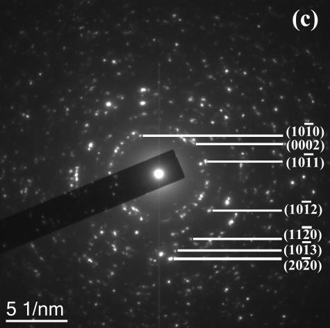
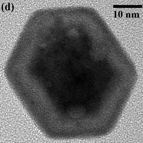
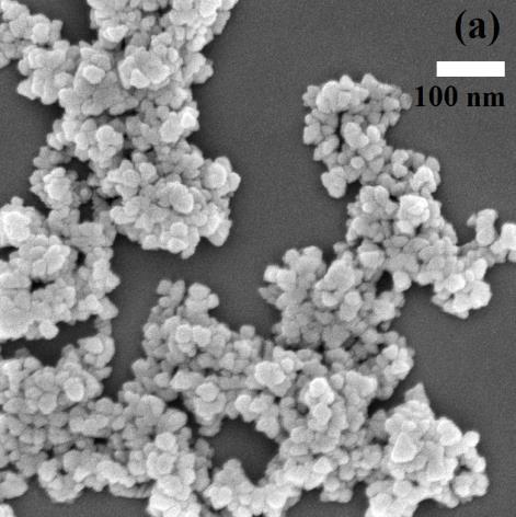
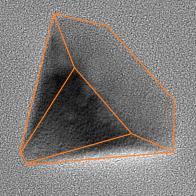
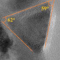
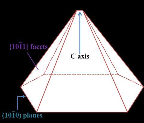
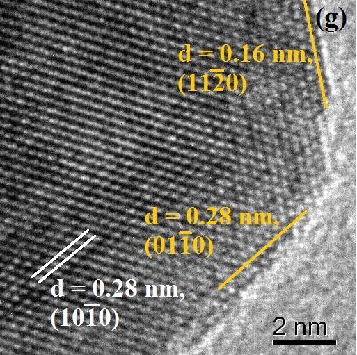
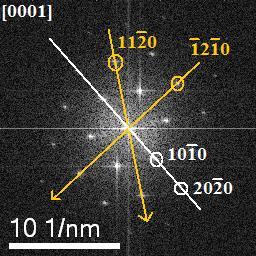
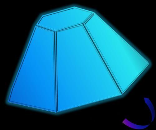
10 Page 9 of 43 In 3+ concentration is observed. This may be due to the imperfect comparison between pure and doped NCs which are not exactly the same size. Furthermore incorporation of dopant ion in interstitial position may result in non-linear trend. Unit cell volume (V) was calculated by using the following equation: (1) The value of V changes from Å 3 to Å 3 with increase of In 3+ doping concentration (ESI, Fig. S8b). The variation of V with In 3+ concentration follows the non-linear trend. Fig. 2a displays the representative field emission scanning electron microscopy (FE- SEM) image of pure ZnO NC. The transmission electron microscopic images at low magnification (Fig. 2b) reveal that hexagonal pyramid shaped ZnO NCs with an average size of 40 nm width and 35 nm height were produced. The top-left and bottom-right insets of Fig. 2b depict the tilted (X = 41.1, Y = 0 ) and side views of a single ZnO hexagonal nanopyramid. The calculated angle between two opposite edges at the tip of the pyramid is 62, and the angle between the edge and the basal plane is 59 as indicated in Fig. 2b. The well defined diffraction spots are indexed to the hexagonal würzite structure (Fig. 2c) consistent with the XRD data. Fig. 2d shows a single hexagonal pyramid viewed from top which also confirms hexagonal nature of the base of NC. Fig. 2e depicts the corresponding selected area electron diffraction (SAED) pattern of the NC which can be indexed as diffractions from [0001] zone axis. The indices of Accepted Manuscript diffraction spots imply that side surfaces of hexagonal pyramid are surrounded by {10 } planes. From SAED pattern and the angle between the edge and basal planes (~ 59 ) of the NC, we conclude that the exposed six surfaces are {10 1} facets. Fig. 2f gives a schematic view of a complete ZnO hexagonal pyramid. The würzite structured ZnO crystal is generally described 9
11 Page 10 of 43 schematically as combination of alternating planes constituted of fourfold tetrahedrally coordinated Zn 2+ and O 2- ions, staking alternatively along the c axis. 18 The Zn 2+ cations rich plane and O 2- anions rich plane form positively charged (0001)-Zn and negatively charged (000 )-O polar surfaces respectively. These two oppositely polar surfaces generate a permanent and spontaneous dipole moment along the c axis and tend to diverge the surface energy. 19,20 Normally most of the ZnO nanostructures grow along the c axis i.e. along the [0001] direction with exposing the six nonpolar {10 0} facets which is parallel to [0001] direction, the polar {0001} and {000 } planes. 21 The nonpolar {10 0} facets are more stable than the parallel polar {0001} and {000 } facets due to the lower surface energy of former one. 22 Besides these two polar surfaces, ZnO has other typical polar surface {10 1}. 23 During the growth of ZnO nanostructures usually {10 0} and {2 0} nonpolar surfaces are the large facets with preferential growth along the c axis rather than polar {0001} surfaces. In our as synthesized ZnO nanopyramid, polar {10 1} facets were the more exposed surface than the nonpolar {10 0} facets although the later facets are thermodynamically more stable. 24 The thermodynamically unstable facets become the more exposed faces due to the predominating kinetic control of reaction system during the growth process. The high energy {10 1} facets are stabilised by proper surface capping of organic molecule which favours the crystal termination on the {10 1} by diminishing the surface energy. The capping molecules compensate the surface charge by the strong electrostatic interaction between the polar surfaces and polar head of capping molecule. Accepted Manuscript Thus the surface energies of basal polar {0001} planes and polar {10 1} planes may decrease in comparison with those other nonpolar faces resulting in a comparatively slow growth rate for these polar planes. 10
12 Page 11 of 43 To understand the exact effect of capping molecule on modification of surface polarity and stabilisation of a particular growth surface, we varied the reaction condition to detect the change in morphology of product. Fig. S9 demonstrates the FTIR spectra of as synthesized ZnO and OLAM. The band at 3342 cm -1 in the IR spectrum of OLAM is due to the N-H stretching mode, which is red shifted and highly broadened at 3436 cm -1 in OLAM capped ZnO NC due to the absorption of N-H groups onto the ZnO surface. The peak at 1583 cm -1 for NH 2 scissoring mode is red shifted to 1596 cm -1 and also broadened. 25 An increase in intensity and broadening of C-N stretching band at 1058 cm -1 confirm the complete surface protection by OLAM. Although amide was a by product in synthesis, as no peak corresponding to amide group was found in IR spectra of as synthesized ZnO, we can conclude only the amine took part in surface capping not the amide or acid group. When OLAM was injected at 240 C instead of very beginning of reaction (90 C) to the reaction solution containing Zn-source and OLAH, the resulted product after 60 mins of reaction is hexagonal platelets with irregular size and shape instead of hexagonal nanopyramid which are depicted in Fig. S10. So OLAM might participate in growth of {10 1} surface. The FT-IR spectra of Zn(acac) 2 and OLAM heated at 90 C are demonstrated in Fig. S3b, which shows that the symmetric and antisymmetric COCC stretching vibrations of Zn(acac) 2 at 1578 cm -1 and 1517 cm -1 are red shifted. 26 This can be due to the formation of Zn(acac) 2 -OLAM complex and the donor NH 2 group sharing its lone-pair of electrons with the Zn 2+ ions. But when OLAM is Accepted Manuscript added at T nu rapid nucleophilic attack of NH 2 takes place at carbonyl centre rather than coordination with Zn 2+ ions, results in rapid growth along stable nonpolar {10 0}surfaces. Due to the lower monomer concentration of nuclei and rapid surface protection by OLAM, platelet structure is formed rather than preferential growth along the c axis. Addition of OLAM at low 11
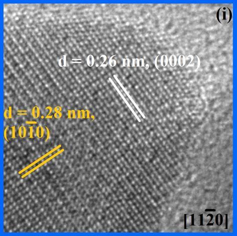
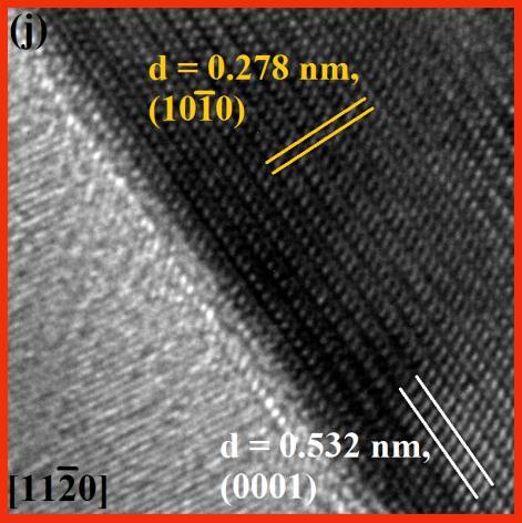
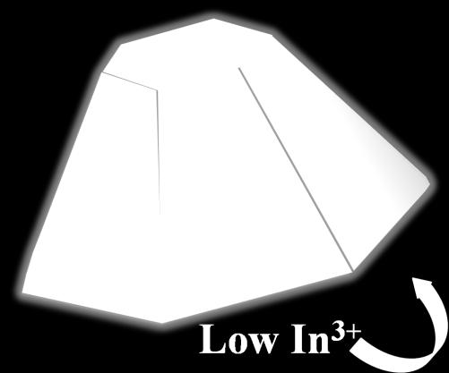
13 Page 12 of 43 temperature leads to consumption of some amount of OLAM by coordination with Zn 2+ in intermediate complex, which gives rise to slow decomposition of the complex and control growth rate of polar {10 1} surfaces. High monomer concentration prefers growth along the c axis. So slow growth rate of ZnO and proper capping by OLAM lead to the formation of beautifully synthesized nanopyramid. Fig. 2g shows the UHRTEM image of a NC captured at the cross-section of two basal edges, which shows surface termination at basal side by (11 0) and (01 0) planes and presence of (10 0) planes parallel to basal edges. The inset at left top depicts the FFT pattern of the corresponding area, which demonstrates the direction of (11 0) and (01 0) planes i.e.; [11 0] and [ 2 0], makes a cross sectional angle of 120 (also it is the angle between two basal edge). The FFT pattern also shows the presence of (10 0) planes. Fig. 2h shows the side view of ZnO NC where the blue and red squared areas are the tip and base of pyramid. HRTEM images of both the area (Fig. 2i and 2j) depict the presence of mutually perpendicular (10 0) and (0002) planes (the zone axis is [11 0]). It is found that the d value of (0002) plane is nearly doubled at base, which is probably due to the high thickness of base; Moiré pattern of crystalline plane is appearing. Figs. S11a to S11c show the TEM images for the ZnIn 2, ZnIn 4 and ZnIn 6. Whereas Fig. S12 depicts the TEM images of ZnIn 8 NC. It is observed that the pyramid height gradually decreases from 35 nm to 11 nm on increasing the In 3+ content leading to the formation of Accepted Manuscript hexagonal platelets. Incorporation of In 3+ into ZnO crystal lattice increases the surface polarity of Zn rich polar surfaces, i.e.; Zn-{0001} and Zn-{10 1} surfaces due to higher electronegativity of In 3+ than Zn 2+. This accretion of surface polarity favours faster electrostatic interaction and consequent surface stabilisation or capping by OLAM onto the Zn-{0001} and Zn-{10 1} 12
14 Page 13 of 43 surfaces. More In 3+ loading leads to more charge accumulation on described surfaces which results in quenching of growth along the c-axis (decrease in pyramid height) and less exposure of {10 1} surfaces. At 8% of In 3+ doping only the hexagonal platelet is formed where {10 1} surface no more exists. Change of basal length is negligible compare to the change of height. Several studies indicate that dopant ions significantly influence nucleation and growth of NCs during synthesis Types of doping i.e. nucleation doping or growth doping depend on growth rate, residence time, morphology and crystal structure. 30 Generally, the nucleated NCs exclude dopant ions from the internal crystal lattice to the surfaces of NCs. Synthetic method in other words growth kinetics limits the maximum doping concentration in colloidal semiconductor NCs. Moreover dopants change the free energy for the stabilization of host crystal structure due to incompatibility in crystal structure and chemical property. 31 Identical decomposition temperature of in-situ formed Zn(acac) 2-x (OLA) x and In(acac)(OLA) 2 precursors and the fast growth rate lead to maximum In incorporation into ZnO NCs. TEM measurements indicate that the size of NC decreases with increase of doping concentration. Thus In dopant ions introduce a thermodynamic potential barrier around the doped ZnO NCs to inhibit NC growth. Internal lattice strain controls the solubility of NCs as described by Gibbs-Thomson relation 27 : (1) Where S r is the solubility of the crystallite of radius r, S B is the solubility of corresponding bulk material, V m is the molar volume, σ is the specific surface energy of Accepted Manuscript nanocrystals. Lattice strain increases continuously with increase of In concentration. Equation (1) suggests that larger strain induces greater crystallite solubility. As a result of it In dopants inhibit the growth of ZnO NCs. 13
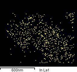
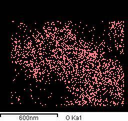
15 Page 14 of 43 To further elucidate the doping status and distribution of In 3+ in ZnIn NCs, systematic characterisations including energy dispersive X-ray spectroscopy (EDS) element mapping and X-ray photoelectron spectra (XPS) were performed. The EDS element mapping of 4% In doped ZnO NCs was carried out to determine the exact position and spatial distribution of dopant ions in the NCs. Fig. 3 shows the HAADF-STEM image of large number of ZnIn 4 NCs which clearly indicate incomplete pyramidal nature of NCs. The EDS element mapping of large number of NCs (in fig. 3) shows that In 3+ ions are homogeneously distributed among the NCs. No phase separation or agglomeration was noticed which concludes that the dopant distribution is quite good. Other two elements Zn and O are also present in nearly stoichiometric ratio and in well distribution. However, the EDS element mapping results cannot verify that the In 3+ ions are located in NCs or on the surface of ZnIn NCs. So fourth, XPS measurements were carried out to further investigate the exact position and binding modes of In 3+ and other elements. Fig. 4 displays the fine scanned Zn2p, O1s and In3d peaks of pure and 4% In doped ZnO samples. The binding energies of Zn 2p 1/2 and 2p 3/2 are around ev and ev respectively with spin-orbit splitting of ev for pure ZnO NCs (Fig. 4a). From the binding energy position, observed spin-orbit splitting value and the highly symmetric nature of high intense peaks, it concludes the presence of Zn as only in the +2 oxidation state in würzite ZnO crystal. 32 The shift of Zn 2p peaks in ZnIn 4 sample toward the lower energies is due to the partial substitution of lattice Zn by In 3+ ions in ZnO and formation of Zn-O-In bonding interaction. Accepted Manuscript Indium is supposed to be present mostly as In 3+ which forms a strong covalent bond with O 2- in doped nanocrystals. Such a strong covalent effect weakens the neighbouring Zn-O bonds and results in decrease of relative positive charge density on Zn ions which causes diminishment of binding energy of Zn 2p peaks. Moreover, the Zn-In interaction i.e. Zn-In bond formation in 14
16 Page 15 of 43 würzite ZnO may cause a decrease in binding energy of Zn 2+ 2p peaks due to smaller difference of electro-negativity between Zn and In compare to Zn and O (Δϰ Zn-In = 0.1, whereas Δϰ Zn-O =1.6, according to Pauling scale). 33 The broadening of peaks is a result of reduced crystalline size and surface plasmon which increases free electron concentration on nanocrystal surface. Fig. 4b demonstrates the O 1s peak of both doped and undoped ZnO NCs. Deconvolution of broad O 1s peak through Peak fit analysis results in a major peak and a sub peak at eV and ev respectively. The lower energy peak is attributed to the O 2- ions in the würzite structure of the hexagonal Zn 2þ ion array. Therefore, the lower energy peak of oxygen spectrum can be attributed to Zn-O bonds. 34 The peak at ev is attributed to O 2- ions in oxygen deficient regions and is related to the presence of oxygen vacancy (V o ). 35 The O 1s peak for ZnIn 4 samples is quite broad and inhomogeneous nature compare to pure one. Deconvolution of fitted curve gives three peaks at ev, ev and ev. Both the crystallite O 2- peak and oxygen vacancy related peaks at ev and ev respectively are significantly broader than that for pure one. Formation of In-O covalent bond changes the effective electric charge on O anion, and the broadness is a mixed effect from In-O and Zn-O bond formation. Large area of the peak related to V o in doped NCs reflects the increase in oxygen vacancy concentration on the nanocrystals surface during the doping. A new hump like peak is appeared at lower energy ( ev) in ZnIn 4 NCs which indicates the presence of oxygen interstitials (O i ). 36 Fig. 4c shows the XPS characteristics peaks for In 3+. Two major peaks at ev and ev are Accepted Manuscript appeared for In3d 3/2 and In3d 5/2 spin-orbit coupling states which is in a very good agreement with the presence of In dopant as In 3+ ion in würzite matrix. 37 Both the peaks somewhat broad and little asymmetric in nature, possibly due to the presence of In 3+ in both in the bulk lattice site and 15
17 Page 16 of 43 surface site. Sharp and smooth natures of In3d peaks also indicate the presence of appreciable amount of In 3+ on the surface of NCs. We carried out absorption spectroscopy to assess the influence on doping to increase the free electron concentration hence change in electronic energy band structure of n-type ZnO host matrix. Fig. 5 shows the absorption spectra of doped and pure ZnO NCs dissolved in TCE in the wavelength range of 300 nm to 3000 nm. All the doped NCs show two strong absorption bands one at UV region and another at near infrared (IR) region. The broad featureless band at IR region can be attributed to surface plasmon absorption of doped NC. The surface plasmon energy decreases with increase of the effective refractive index of the sample by the addition of high refractive index solvent. (Fig. S22) The plasmonic absorbance at IR region is confirmed by the observation of shifting of plasmonic band with solvent variation. The excess electron created in the system due to n-type doping can resonance in the confined dimension of NC. The resonance excitation of this plasmon by electromagnetic radiation results in the absorbance at IR region. The IR absorption intensity increases monotonically with the increase of In 3+ doping concentration. We cannot collect the absorbance nature beyond 3000 nm for the instrument limitation and appearance of noise due to the vibrational overtones of solvent molecules. To get the clear nature of IR absorbance by NCs, we performed FT-IR spectroscopy with the powdered sample which will be discussed in later paragraph. The plasmon band appeared at IR region is an effect of presence of free electrons in the Accepted Manuscript conduction band. The modified Drude-Lorentz model can quantitatively explain this phenomenon. 38 According to this model there is a direct proportional relationship between the absorption coefficient (α) of free electron in semiconductor and the charge carrier density (N) as follows: 16
18 Page 17 of 43 (2) where c and ω are the speed and frequency of incident light, e is the electron charge, m* is the effective mass of an electron, ε 0 is the vacuum permittivity, τ is the mean time between two electron scattering events, n is the refractive index of pure semiconductor. Furthermore according to Mie s theory, 39 the energy position of plasmon band is related to the surface plasmon resonance frequency (ω p ) which is proportional to the square root of the free electron concentration: ω p = (3) Where ε opt is the dielectric constant measured in the transparent region of the spectrum of a pure semiconductor sample. It is very clear from the nature of IR absorbance of samples as depicted in Fig. 5 that the plasmon band absorption maximum (normalised with respect to band gap absorbance) increases with increasing of In 3+ doping concentration due to gradual increase of free electron concentration, also quite expected according to equation (2). The IR absorbance of ZnIn 8 NC (in Fig. 6) is found to be broader compare to other doped NC along with reduction in absorbance intensity compare to ZnIn 6 (Fig. 5). This behaviour may be a result of inhomogeneous doping, electron trapping around In 3+ sites 40 and destruction of particle size distribution. Fig. 6 shows the change of plasmon band energy with the variation of In 3+ doping Accepted Manuscript concentration. The broad surface plasmon resonance peak shifts to higher energy on increasing doping concentration suggesting an increase in the amount of free carriers. Based on equation (3) and taking the optical parameter values (m * = 0.24 m 0 and ε opt = 7.77) for bulk würzite ZnO system, 41 the concentration of free electron is found to be cm -3, cm -3, cm -3, cm -3 and cm -3 for 1%, 2%, 4%, 6% and 8% In 3+ doped 17
19 Page 18 of 43 NCs respectively. These values are comparable with previous reported values for In or Ga doped ZnO films. 42,43 The change of plasmon energy and free electron concentration are in agreement with Drude s model for the free electron gas formation in semiconductors. Besides the modification of surface plasmon resonance in IR region there is a continuous change of band gap of ZnIn NC. The optical band gap of ZnIn NC with different In loading was determined from differential absorbance spectra (da/dλ vs.λ) 44 shown in Fig. S14. A progressive blue shift of band gap is observed on increasing doping percentage. Introduction of In 3+ dopant into the ZnO matrix creates free electrons which generally accumulate at the bottom of conduction band resulting in an increase of band gap. This phenomenon is known as Burstein- Moss (BM) effect As our synthesized NCs are not in quantum confinement region so the amplification of band gap is solely attributed to the BM effect. The resulting band gap from derivative plot is summarised in Table 2 which shows an increase of band gap from ev (for pure one) up to ev (for ZnIn 6 NCs). The increase in the Fermi level in the conduction band of the degenerate semiconductor leads to an energy gap widening effect. According to the BM effect, broadening of the optical band gap can be expressed as follows: 48 ΔE BM = ( ) 3 (4) Where = + In which ΔE BM is the energy band gap broadening, is the reduced Planck constant, μ is Accepted Manuscript the effective mass of the carrier, N is the carrier concentration, and are the effective mass of hole and electron with the value 0.28m 0 and 0.59 m 0 ( m 0 = free electron mass) respectively. 49 According to this equation band gap increases with carrier concentration. The electron concentration (N) calculated from equation (4) for different In 3+ concentrations is summarised in 18
20 Page 19 of 43 Table 2. The N values calculated from equation (4) are very similar to that found using Mie s theory where ω p is the experimental quantity. It suggests that doping process is very homogenous and might create similar effect on band gap and plasmonic frequency enhancement. The little lower value in magnitude of N using BM effect is found probably due to the negligence of dielectric constant of medium. There is a decrease in band gap as well as electron concentration (calculated from BM effect) for ZnIn 8 compare to ZnIn 6. At higher concentration of doping, In 3+ introduces some localised states of energy into the ZnO band structure which can interact with conduction band. This interaction leads to mixing and anticrossing of these bands which results a gap in the conduction band with perturbed bands of energy (destruction of parabolic nature of conduction band). Therefore, the magnitude of the E g is reduced when the optical transition promotes electrons from the valence band to states in the conduction band close to the new gap (Scheme II C). 50,51 Even at higher doping concentration ca. 6% the NC remain highly transparent in visible range which is clear from absorption spectra and photograph of hexane solution of NCs (ESI, Fig. S15). When we tried to dope beyond 6% there was no much change in band gap but a little decrease of IR absorbance intensity was observed. The decrease of IR absorbance peak intensity for ZnIn 8 may be a result from localisation of electron charge around the cations and scattering with impurity ions. 3 Although the solid solution limit for In 3+ in ZnO by our synthetic strategy is 8% as concluded from XRD analysis but superior plasmon property is observed up to ca. 6%. Accepted Manuscript To know details about the change of optical property upon In 3+ doping in ZnO matrix steady state photoluminescence spectroscopy was performed. A summary of PL profile of doped and pure samples is presented in Fig.7. Normally the PL profile of ZnO based nanocrystal shows two types of emission: near band edge emission (NBE) and deep level emission (DLE). The 19
21 Page 20 of 43 NBE emission which appears in UV region (nearly nm) upon excitation with 330 nm for all the NCs is attributed to the radiative recombination of photo generated holes in the valence band and electrons in the conduction band i.e. the excitonic recombination. The pure ZnO NC has an intense ultra violet peak with a defect related photoluminescence peak centred at 495 nm. The green emission centred at 495 nm may be due to the (i) recombination of photo generated electrons in conduction band with the deep state defect levels (V o, V Zn, O i, Zn i or O Zn which is situated very close to the valence band) or (ii) recombination of electron in shallow trap state (mainly Zn i states) with the deep defects states. Where V o and V Zn stands for oxygen and Zinc vacancy respectively. O i and Zn i means interstitial O and Zn atom. O Zn stands for oxygen atom in Zn lattice site It is found that the intensity of green emission peak has higher intensity than UV emitting peak for pure ZnO. XPS analysis for ZnO NC confirms (in Fig.4b) the presence of oxygen vacancy on the NCs surface and no trace of O i (which generally appears at lower binding energy than pure O1s peak). So in pure sample only oxygen vacancy related defect states like V o, V + o or V ++ o are expected as the deep trap states and recombination of electron from conduction band to V o generates the green emission. However for the doped NCs on increasing doping concentration the green emission peak decreases and high energy peaks at 398 nm, 422 nm and 449 nm become intensified. This indicates a higher band to band recombination and shallow states to valence band recombination with the consequence diminution of radiative transition due to oxygen vacancy. Also a little red shift in V o related Accepted Manuscript emission peak was observed. It indicates that In 3+ doping in ZnO greatly affect the defect equilibrium resulting in the change in the concentration of different types of defects in ZnO NCs. From the literature it is very clear that PL peak related to O i defects appears at higher wavelength (560 nm) than that V o defects ( nm). 55,56 The introduction of In 3+ in ZnO matrix 20
22 Page 21 of 43 promotes the oxygen diffusion in ZnO matrix 57 which leads to the suppression of oxygen vacancies (V O ) related defects and consequence creation of oxygen interstitials (O i ) defects. Thus, the presence of In 3+ in ZnO matrix decreases the contribution of V O related PL peak (by neutralising some of the V o states) and increases the contribution of O i related PL peak. The overall PL spectra are expected to show a red shift in In-doped ZnO NCs as compared to the undoped ZnO NCs. XPS analysis of O 1s peak of ZnIn 4 NC reveals the presence of interstitial oxygen (O i ) along with oxygen vacancy which supports our speculation regarding the presence of O i and involvement in luminescence process. Beside the change of oxygen vacancy related PL peak intensity the other emission peaks at 397nm, 421 nm and 449 nm also get altered on changing doping percentage. The blue emission in ZnO system generally appears due to the presence of interstitial Zn atoms (Zn i ). 58 A gradual increase of doping % blue emission peak at 421 nm and 449 nm gets intensified than the band edge emission and consequence loss of green emission. The blue emission centred at 421 nm is observed for all the samples including the pure one. The overlap of band edge emission with blue emission for ZnO and ZnIn 1 NCs indicates that the Zn i defect related levels are very closely situated to the bottom of conduction band. Whereas for ZnIn 2 to ZnIn 6 nanocrystal distinct nature of violet emitting and blue emitting peaks gradually appear which may be a result of increase of Zn i concentration in the systems. The presence of Zn i can be concluded by analysing the Zn LMM Auger peak which is often used to identify the chemical states of the zinc species. 59 Auger peaks usually show larger shape changes Accepted Manuscript than XPS peaks with varying chemical states because a single Auger transition involves three electrons and many body effects. Fig. S16 shows the typical Auger Zn L 3 M 4,5 M 4,5 spectrum of the ZnIn 4 NC. This spectrum is Gaussian fitted with two Auger peaks centred at ev and ev which are attributed to the interstitial zinc (Zn i ) and Zn-O bonds respectively. 21
23 Page 22 of 43 Strikingly all the PL emission intensities for the defect related emission of In doped ZnO NCs are much lower than the pure one. The appearance of surface plasmon band in doped NCs may oppose normal electron-hole recombination at the surface by reducing the separation of electron and holes within the surface depletion region. 60 Anomalous behaviour for ZnIn 8 NCs is found where only the UV emission is observed with total suppression of visible emission. The formation of an amorphous layer of In 2 O 3 on ZnIn 8 NCs may responsible for this abnormal behaviour which quench the visible emission (also affects the plasmonic property of ZnIn 8 NCs) as it forms an insulator barrier on the NC surface. 61,62 The schematic diagram (scheme II) depicts a fair idea about the luminescence process. For the successful practical application of the NCs, it is very necessary to deposit the NCs as a film by preserving the optical and electrical properties. In situ ligand exchange process 63 was performed to remove nonconductive organic ligand (OLAM) by formic acid. The as-prepared film was immersed in 0.1 (M) formic acid solution in acetonitrile for 5 mins. The surface of ligand exchanged film was mildly washed with ethanol and dried under vacuum. Finally the film was annealed at 300 C for 2 hrs to remove the formic acid. Fig. S18a and S18b shows the crosssectional and top view of as-deposited film of ZnIn 4 NCs. Whereas Fig. S18c describes the cross-section view of ligand exchanged film which shows a homogenous film formation and Fig. S18d shows the top view which gives a fair idea about the absence of cracks in the film. The films are completely transparent in the visible region (transparency ~ 95%) and the inherent Accepted Manuscript surface plasmon peak remains unchanged after ligand exchange (Fig. S19). Sufficient care was taken during the ligand exchange process as excess exposure of formic acid (exposure time more than 10 mins or high concentration of formic acid) results in high decrease in surface plasmon peak intensity due to corrosion of NC s surface by formic acid. 22
24 Page 23 of 43 In order to trace the conductive properties of the as annealed films, temperature dependent resistance was measured by conventional two probe method. Fig. 8 shows the variation of sheet resistance of films at temperature range 80 K to 300 K with different In 3+ concentrations. Pure ZnO film shows relatively high room temperature (RT) sheet resistance (ρ) ~ 53.2 KΩ/sq. and a negative temperature coefficient of resistivity (TCR), characteristic of semiconductor behaviour. A clear decrease in sheet resistance of ~1.5 orders of magnitude (2 KΩ/sq.) has been observed for 1% In 3+ doped film. Gradual increase of dopant % decreases the RT sheet resistance up to 740 Ω/sq for 6% indium doping, which reaches state of art performance of ITO colloidal coatings after annealing 64 and Ga doped ZnO coatings from colloidal inks. 5 The most interesting characteristic feature for ZIO films is that they show metalsemiconductor (MST) transition at low temperature. The MST transition temperature (T s ) varies from 250 K to 105 K with increasing In concentration. The positive value of TCR above the T s and negative value below the T s reflects two different conduction mechanisms are compete each other. Such behaviour in temperature dependence of resistance is common in TCO films such as Ga and Al doped ZnO, 65 Nb and La doped SrTiO 66,67 3 and La-doped BaSnO The decrease in sheet resistance and appearance of metal like conductivity can be explained by the increase in carrier concentration and formation of degenerate band due to In doping. Increase in n-type doping in the system gives rise to gradual filling up of the bottom state of conduction band and consequent shifting of Fermi level towards the conduction band results in the metallic behaviour. Accepted Manuscript For 2, 4 and 6% In doped films, contribution from metallic conduction process increases as the T s shifts lower temperature. Beside the metallic conduction, below T s the conduction process is mainly governed by variable range hopping process (VRH) in doped semiconductors. Excellent linear fit of ln(ρt -1/2 ) vs. T -1/4 plot (below T s ) supports VRH conduction process. 69 So 23
25 Page 24 of 43 the In doping introduces degenerate semiconductor nature in wide band gap ZnO system which reflects metallic conductivity at room temperature. On the other hand it decreases the acceptor impurity (also confirmed from PL emission) which facile the VRH mechanism to be the predominate one. Abnormal behaviour in conductivity is found for ZnIn 8 film where the RT sheet resistance is higher than the other doped films, and the negative TCR value confirms the semiconductor behaviour. The dominant conduction is VRH process for ZnIn 8 film. The best conductive film ZnIn 6 shows very low sheet resistance upon thermal annealing. Sheet resistance is dropped from 740 Ω/sq. to 120 Ω/sq. on annealing at 700 C. This is the best report till date for sheet resistance of ZnO based TCO films and very close to commercially available ITO glass slide (~ 40 Ω/sq for Sigma-Aldrich, cat. No ). The transparency in visible region is somewhat reduced to 70% for the formation of oxygen and indium vacancies. The synthesis protocol as we discussed is very useful also for synthesizing Al 3+ and Ga 3+ ZnO colloids (ESI, Fig.S21) taking the dopant precursor as acetylacetonate complex. Further extensive studies regarding TCO properties of Al 3+ and Ga 3+ doped ZnO colloids are currently underway in our laboratory. Conclusion: In summary, we successfully synthesized In doped ZnO colloidal NCs by thermal decomposition of metal carboxylate salt and studied the effect of dopant source on doping percentage in host matrix. Sizes of In doped ZnO NCs decrease upon In doping which indicate Accepted Manuscript that dopant impurities inhibit NC growth in solution. The effect of n-type doping in ZnO matrix on band structural change and various types of vacancy states has been thoroughly investigated from absorbance and PL spectroscopy. The doped NC shows excellent plasmonic property in near infrared region. Cost effective high quality film can be easily produced by spin casting and 24
26 Page 25 of 43 in situ ligand exchange process. The doped ZnO NCs reveal metal-semiconductor transition at low temperature. The higher electrical conductivity of ZIO films concomitant with the visible range transparency and good plasmonic property makes the ZIO NCs a superior substitute of costly ITO films and a promising candidate of plasmonic materials. Acknowledgement: The authors Sirshendu Ghosh and Manas Saha are thankful to Council of Scientific and Industrial Research (CSIR), Govt. of India for providing the fellowship during the tenure of the work. The authors acknowledge Dr. Vishal Dev Ashok and Babusona Sarkar for their useful suggestions. Accepted Manuscript 25
27 Page 26 of 43 Table 1: Composition analysis of In 3+ doped ZnO nanocrystals for different indium sources by ICP-AES and EDS analysis. Mole (%) In precursor ICP-AES (mole %) EDS (mole %) In(acac) In(Oac) In(acac) In(Oac) In(acac) In(Oac) In(acac) In(Oac) In(acac) In(Oac) Accepted Manuscript 26
28 Page 27 of 43 Table 2: Optical band gap energy (E g ), plasmon wavelength (λ p ), electron concentration (N) calculated from BM effect and Mie s theory for ZnO nanocrystals with different In doping contents. Doping (%) ZnO (0%) ZnIn 1 O (1%) ZnIn 2 O (2%) ZnIn 4 O (4%) ZnIn 6 O (6%) ZnIn 8 O (8%) E g [ev] λ p (nm ) N [cm -3 ] X10 19 (Burstein Mass effect) N [cm -3 ] X10 19 (Mie s theory) Accepted Manuscript 27
29 Page 28 of 43 References: (1) Ginley, D. S.; Hosono, H.; Paine, D. C. Handbook of Transparent Conductors; Springer: New York, (2) Wan, Q.; Dattoli, E. N.; Lu, W. Appl. Phys. Lett. 2007, 90, (3) Wang, T.; Radovanovic P. V. J. Phys. Chem. C 2011, 115, (4) Buonsanti, R.; Llordes, A.; Aloni, S.; Helms, B. A.; Milliron, D. J. Nano Lett. 2011, 11, (5) Gaspera, E. D.; Bersani, M.; Cittadini, M.; Guglielmi, M.; Pagani, D.; Noriega, R.; Mehra, S.; Salleo, A.; Martucci, A. J. Am. Chem. Soc. 2013, 135, (6) Serin, T.; Yildiz, A.; Uzun, Ş.; Çam, E.; Serin, N. Phys. Scr. 2011, 84, (6pp). (7) Gordon, T. R.; Paik, T.; Klein, D. R.; Naik, G. V.; Caglayan, H.; Boltasseva, A.; Murray, C. B. Nano Lett. 2013, 13, (8) Trizio, L. D.; Buonsanti, R.; Schimpf, A. M.; Llordes, A.; Gamelin, D. R.; Simonutti, R.; Milliron, D. J. Chem. Mater. 2013, 25, (9) Nozik, A. J. Phys. Rev. B 1972, 6, (10) Coutts, T. J.; Young, D. L.; Li, X.; Mulligan, W. P.; Wu, X. J. Vac. Sci. Technol. A 2000, 18, (11) Wang, A.; Babcock, J. R.; Edleman, N. L.; Metz, A. W.; Lane, M. A.; Asahi, R.; Dravid, V. P.; Kannewurf, C. R.; Freeman, A. J.; Marks, T. J. Proc. Natl. Acad. Sci. 2001, 98, Accepted Manuscript (12) Bhosle, V.; Narayan, J. J. Appl. Phys. 2006, 100, (13) Hwang, D-K.; Oh, M-S.; Lim, J-H.; Park, S-J. J. Phys. D: Appl. Phys. 2007, 40, R387 R
30 Page 29 of 43 (14) Li, L.; Hutter, T.; Finnemore, A. S.; Huang, F. M.; Baumberg, J. J.; Elliott, S. R.; Steiner, U.; Mahajan, S. Nano Lett. 2012, 12, (15) Kumar, V.; Singh, R.G.; Purohit, L.P.; Mehra, R.M. J. Mater. Sci. Technol. 2011, 27, (16) Fang, T-H.; Kang, S-H. Curr. Appl. Phys. 2010, 10, (17) Li, D. P.; Wang, G. Z.; Han, X. H. J. Phys. D: Appl. Phys. 2009, 42, (18) Wang, Z. L.; Kong, X.Y.; Zuo, J. M. Phys Rev Lett. 2003, 91, (19) Wang, Z. L. J. Phys.: Condens. Matter 2004, 16, R829 R858. (20) Yang, M.; Sun, K.; Kotov, N. A. J. Am. Chem. Soc. 2010, 132, (21) Xu, L.; Guo, Y.; Liao, Q.; Zhang, J.; Xu, D. J. Phys. Chem. B 2005, 109, (22) Meyer, B.; Marx, D. Phys. Rev. B 2003, 67, (23) Wang, Z. L.; Kong, X. Y.; Ding, Y.; Gao, P. X.; Hughes, W. L.; Yang, R. S.; Zhang, Y. Adv. Funct. Mater. 2004, 14, 943. (24) Yang, R. S.; Ding, Y.; Wang, Z. L. Nano Lett. 2004, 4, (25) Shukla, N.; Liu, C.; Jones, P. M.; Weller, D. J. Magn. Magn. Mater. 2003, 266, 178. (26) Bahers, T. L.; Pauporté, T.; Labat, F.; Lefevre, G.; Ciofini, I. Langmuir 2011, 27, (27) Schwartz, D. A.; Norberg, N. S.; Nguyen, Q. P.; Parker, J. M.; Gamelin, D. R. J. Am. Chem. Soc.2003, 125, Accepted Manuscript (28) Farvid, S. S.; Dave, N.; Wang, T.; Radovanovic, P. V. J. Phys. Chem. C 2009,113,15928 (29) Feng, J.; Zhu, H.; Yang, X. 2013, 5,6318. (30) Erwin, S. C.; Zu, L.; Haftel, M. I.; Efros, A. L.; Kennedy, T. A.; Norris, D. J. Nature 2005, 436,
31 Page 30 of 43 (31) Oxtoby, D. W.; Acc. Chem. Res., 1998, 31 (2), 91. (32) Crist, P. D. B. V. Handbook of The Elements and Native Oxides(XPS International, Inc., 1999), Vols. 1 and 2. (33) Ilyas, U.; Rawat, R. S.; Tan, T. L.; Lee, P.; Chen, R.; Sun, H. D.; Fengji, L.; Zhang, S. J. Appl. Phys 2012, 111, (34) Tay, Y. Y.; Li, S.; Sun, C. Q.; Chen, P. Appl. Phys. Lett. 2006, 88, (35) Ghosh, S.; Das, K.; Sinha, G.; Lahtinen, J.; De, S. K. J. Mater. Chem. C 2013, 1, (36) Liu, W.; Li, W.; Hu, Z.; Tang, Z.; Tang, X. Appl. Phys. Lett. 2011, 110, (37) Sarath Kumar, S. R.; Hedhili, M. N.; Alshareef, H. N.; Kasiviswanathan, S. Appl. Phys. Lett. 2010, 97, (38) Fox, M. Optical Properties of Solids; Oxford University Press: NewYork, (39) Mulvaney, P.; Liz-Marzan, L. M.; Giersig, M.; Ung, T. J. Mater. Chem. 2000, 10, (40) Kanehara, M.; Koike, H.; Yoshinaga, T.; Teranishi, T. J. Am. Chem. Soc. 2009, 131, (41) Baer, W. S. Phys. Rev.1967, 154, 785. (42) Lin, W.; Ding, K.; Lin, Z.; Zhang, J.; Huang, J.; Huang, F. CrystEngComm, 2011, 13, Accepted Manuscript (43) Hammarberg, E.; Prodi-Schwab, A.; Feldmann, C. J. Coll. Int. Sc.2009, 334, 29. (44) Ellingson, R. J.; Beard, M. C.; Johnson, J. C.; Yu, P.; Micic, O. I.; Nozik, A. J.; Shabaev, A.; Efros, A. L. Nano Lett. 2005, 5, (45) Mridha, S.; Basak, D. J. Phys. D: Appl. Phys. 2007, 40,
32 Page 31 of 43 (46) Lu, J. G.; Fujita, S.; Kawaharamura, T.; Nishinaka, H.; Kamada, Y.; Ohshima, T.; Ye, Z. Z.; Zeng, Y. J.; Zhang, Y. Z.; Zhu, L. P.; He, H. P.; Zhao, B. H. J. Appl. Phys. 2007, 101, (47) Suwanboon, S.; Amornpitoksuk, P.; Haidoux, A.; Tedenac, J. C.J. Alloys Compd. 2008, 462, (48) Sernelius, B.; Berggren, K. F.; Jin, Z. C.; Hamberg, I.; Granqvist, C. Phys. Rev. B 1988, 37, (49) Chen, R.; Zhu, P.; Zhao, T.; Fu, X.; Zhou, F.; Sun, R. Eur. J. Inorg. Chem. 2013, 20, (50) Sans, J. A.; Sánchez-Royo, J. F.; Segura, A.; Tobias, G.; Canadell, E. Phys. Rev B 2009, 79, (51) Jia, J.; Takasaki, A.; Oka, N.; Shigesatoa, Y. J. Appl. Phys.2012, 112, (52) Wena, F.; Li, W.; Moona, J-H.; Kim, J. H. Solid State Communications 2005, 135, 34. (53) Vanheusden, K.; Warren, W. L.; Seager, C. H.; Tallant, D. R.; Voigt, J. A. J. Appl. Phys.1996, 79, (54) Shi, Y.L.; Wang, J.; Li, H.L. Appl. Phys. A 2004, 79, (55) Kurbanov, S.S.; Panin, G.N.; Kim, T.W.; Kang, T.W. J. Lumin. 2009, 129, (56) Hsu, J.W.P.; Tallant, D.R.; Simpson, R.L.; Missert, N.A.; Copeland, R.G. Appl. Phys. Lett. 2006, 88, (57) Ryoken, H.; Sakaguchi, I.; Ohashi, N.; Sekiguchi, T.; Hishita, S.; Haneda, H. J. Mater. Accepted Manuscript Res.2005, 20, (58) Zeng, H.; Duan, G.; Li, Y.; Yang, S.; Xu, X.; Cai, W. Adv. Funct. Mater. 2010, 20, (59) Wolan, J. T.; Horflund, G. B. Appl. Surf. Sci.1998, 125,
33 Page 32 of 43 (60) Cheng, C. W.; Sie, E. J.; Liu, B.; Huan, C. H. A.; Sum, T. C. Appl. Phys. Lett. 2010, 96, (61) Richters, J-P.; Voss, T.; Kim, D S.; Scholz, R.; Zacharias, M. Nanotechnology 2008, 19, (62) Richters, J-P.; Voss, T.; Wischmeier, L.; Rückmann, I.; Gutowski, J. Appl. Phys. Lett. 2008, 92, (63) Zarghami, M. H.; Liu, Y.; Gibbs, M.; Gebremichael, E.; Webster, C.; Law, M. ACS Nano 2010, 4, (64) Lee, J.; Lee, S.; Li, G.; Petruska, M. A.; Paine, D. C.; Sun, S. J. Am. Chem. Soc. 2012, 134, (65) Han, J. P.; Mantas, P. Q.; Senos, A. M. R. in 7th International Conference on Electronic Ceramics and Their Applications (ELECTROCERAMICS VII-2000)(Elsevier Science Ltd, Portoroz, Slovenia, 2000), p (66) Ramadan, W.; Ogale, S. B.; Dhar, S.; Zhang, S. X.; Kundaliya, D. C.; Satoh, I.; Venkatesan, T. Appl. Phys. Lett.2006, 88, (67) Cho, J. H.; Cho, H. J. Appl. Phys. Lett. 2001, 79, (68) Liu, Q.; Liu, J.; Li, B.; Li, H.; Zhu, G. Appl. Phys. Lett 2012, 101, (69) Mott, N. F.; Davis, E. A. Electronic processes in non-crystalline materials, 2 nd ed. (clarendon, oxford, 1979). Accepted Manuscript 32
34 Page 33 of 43 Figure captions: Fig. 1. (a) XRD patterns of pure and doped ZnO nanocrystals ZnIn 1, ZnIn 2, ZnIn 4, ZnIn 6 and ZnIn 8. (b) change of lattice parameter and strain with In doping. Fig. 2. (a) FESEM image of pure ZnO.(b) Low resolution TEM image of pure ZnO nanopyramid. The top-left and bottom right insets of Figure depicts the tilted (X = 41.1, Y = 0 ) and side views of a single ZnO hexagonal nanopyramid. (c) SAED pattern of nanopyramid. (d) A single hexagonal pyramid viewed from (0001) zone axis. (e) SAED pattern of single nanocrystal. (f) Schematic presentation of a nanopyramid. (g) HRTEM image of a nanocrystal at the cross-section of two edge of base. Inset shows the corresponding FFT pattern of the area. (h) Side view of a nanopyramid. (i) HRTEM image of tip of pyramid. (j) HRTEM image of base of pyramid. Fig. 3. STEM dark field image and EDS element mapping of Zn, In and O. Fig. 4. XPS spectra of (a, b) the pure and ZnIn 4 samples for Zn 2p and O 1s peaks respectively; (c) the In 3d peaks for ZnIn 4 sample. Fig. 5. Optical absorbance of all ZnIn samples in Vis-NIR region normalised with respect to band gap absorbance. Fig. 6. FTIR spectra of ZnIn samples in solid form with different amount In loding. The extra sharper peaks is due to the organic ligand absorbed on nanocrystal s surface. Fig. 7. PL profile of ZnIn samples at different In concentration. Accepted Manuscript Fig. 8. Temperature dependent sheet resistance of (a) pure ZnO, (b) ZnIn 1, (c) ZnIn 2, (d) ZnIn 4, (e) ZnIn 6 and (f) ZnIn 8. Scheme I: shape transformation of ZnIn nanocrystals on increasing In loading. 33
35 Page 34 of 43 Scheme II: Schematic presentation of band structure and interstitial defects of (A) pure ZnO, (B) ZnO at moderate doping concentration (2, 4 and 6 mole%), (C) ZnIn 8 sample; E LS is the localised state due to excess In 3+ and E LS / is the deformed localised state (LS) after interaction with conduction band (E c ). E F is flattened conduction band after interaction with LS.. Accepted Manuscript 34
36 Expansion (%) (100) (002) (101) (102) (110) (103) (201) (004) Intensity (a.u.) Lattice strain Page 35 of 43 Figures: (a) ZnIn 8 ZnIn a expansion c expansion 2 (degree) Indium (%) A Fig. 1 ZnIn 4 ZnIn 2 ZnIn 1 ZnO (b) 2.5x x x x x Accepted Manuscript 35


37 Page 36 of 43 Accepted Manuscript Fig. 2 36

38 Page 37 of 43 Accepted Manuscript Fig. 2 37

39 Page 38 of 43 Accepted Manuscript Fig. 3 38
40 Counts (a.u.) Counts (a.u.) Counts (a.u.) Page 39 of 43 Zn2P Zn2P 1/2 3/ ZnIn ZnO Binding energy (ev) (a) ZnIn 4 In3d 5/2 In3d 3/2 ZnIn ev ev ev ZnO ev ev Binding energy (ev) (c) (b) Accepted Manuscript Binding Energy (ev) Fig. 4 39
41 Abs (a. u.) Page 40 of 43 ZnIn 8 ZnIn 6 ZnIn 4 ZnIn 2 ZnIn 1 ZnO (nm) Fig. 5 Accepted Manuscript 40
42 PL Intensity (a.u.) Transmittance (%) Page 41 of 43 ZnIn 1 ZnIn 2 ZnIn 4 ZnIn 6 ZnIn Wavenumber (cm -1 ) Fig. 6 ZnO ZnIn 1 ZnIn 2 ZnIn ZnIn 6 Accepted Manuscript ZnIn Wavelength (nm) Fig. 7 41
43 Sheet rasistance (Ohm/sq.) Sheet resistance (KOhm/sq.) ln( T -1/2 ) Sheet resistance (KOhm/sq.) ln( T -1/2 ) Sheet resistance (Ohm/sq.) ln( T -1/2 ) Sheet resistance (KOhm/sq.) ln Sheet resistance (KOhm/sq.) ln Page 42 of (c) (a) 14.4 Variable range hopping T = 200K Linear fit /T (K -1 ) ZnO T (K) Linear Fit T -1/4 (K -1/4 ) ZnIn 2 T s = 205 K (e) T s = 105K T (K) (b) (d) 11 Variable range hopping below 200K Linear fit /T (K -1 ) T ZnIn s = 250K (f) T (K) T -1/4 (K -1/4 ) Linear Fit T ZnIn s = 140K T (K) T -1/4 (K -1/4 ) Linear fit Accepted Manuscript T (K) ZnIn ZnIn T (K) Fig. 8 42


44 Page 43 of 43 Scheme-I Accepted Manuscript Scheme - II 43
Tunable surface plasmon resonance and enhanced electrical. conductivity of In doped ZnO colloidal nanocrystals
 Electronic Supplementary Material (ESI) for Nanoscale. This journal is The Royal Society of Chemistry 2014 Abs (normalised) Electronic Supplementary Information : Tunable surface plasmon resonance and
CHAPTER 6. BLUE GREEN AND UV EMITTING ZnO NANOPARTICLES SYNTHESIZED THROUGH A NON AQUEOUS ROUTE
 71 CHAPTER 6 BLUE GREEN AND UV EMITTING ZnO NANOPARTICLES SYNTHESIZED THROUGH A NON AQUEOUS ROUTE 6.1 INTRODUCTION Several techniques such as chemical vapour deposition, electrochemical deposition, thermal
CHAPTER 8 SUMMARY AND FUTURE SCOPE
 CHAPTER 8 SUMMARY AND FUTURE SCOPE The potential of room temperature ferromagnetism in many diluted magnetic semiconductors has opened up a new route for realization of spintronic devices. Based on the
CHAPTER 3. EFFECT OF PRASEODYMIUM DOPING ON THE STRUCTURAL AND OPTICAL PROPERTIES OF ZnO NANORODS
 46 CHAPTER 3 EFFECT OF PRASEODYMIUM DOPING ON THE STRUCTURAL AND OPTICAL PROPERTIES OF ZnO NANORODS 3.1 INTRODUCTION Zinc oxide, one of the most promising materials, has been demonstrated to be applicable
CHAPTER 8 SYNTHESIS, STRUCTURAL, OPTICAL AND ELECTRICAL PROPERTIES OF. TRANSITION METAL (TM) DOPED ZnO NANORODS. (TM=Mn, Co, Ni AND Fe).
 DOPED ZnO NANORODS. (TM=Mn, Co, Ni AND Fe).") 190 CHAPTER 8 SYNTHESIS, STRUCTURAL, OPTICAL AND ELECTRICAL PROPERTIES OF TRANSITION METAL (TM) DOPED ZnO NANORODS (TM=Mn, Co, Ni AND Fe). 8.1 Introduction The important and fundamental work for developing
190 CHAPTER 8 SYNTHESIS, STRUCTURAL, OPTICAL AND ELECTRICAL PROPERTIES OF TRANSITION METAL (TM) DOPED ZnO NANORODS (TM=Mn, Co, Ni AND Fe). 8.1 Introduction The important and fundamental work for developing
Structural, Optical & Surface Morphology of Zinc Oxide (ZnO) Nanorods in Molten Solution
 Nanorods in Molten Solution") Journal of Materials Science and Engineering B 6 (3-4) (2016) 68-73 doi: 10.17265/2161-6221/2016.3-4.002 D DAVID PUBLISHING Structural, Optical & Surface Morphology of Zinc Oxide (ZnO) Nanorods in Molten
Journal of Materials Science and Engineering B 6 (3-4) (2016) 68-73 doi: 10.17265/2161-6221/2016.3-4.002 D DAVID PUBLISHING Structural, Optical & Surface Morphology of Zinc Oxide (ZnO) Nanorods in Molten
Annealing Influence on the Optical Properties of Nano ZnO
 Available online www.ejaet.com European Journal of Advances in Engineering and Technology, 2014, 1(1): 69-73 Research Article ISSN: 2394-658X Annealing Influence on the Optical Properties of Nano ZnO Saad
Nanostructured ZnO as a solution-processable transparent electrode material for low-cost photovoltaics
 Nanostructured ZnO as a solution-processable transparent electrode material for low-cost photovoltaics Investigators P.I: Alberto Salleo, Assistant Professor, Materials Science and Engineering Dr. Ludwig
PREPARATION AND CHARACTERIZATION OF METAL OXIDE NANOPOWDERS BY MICROWAVE- ASSISTED COMBUSTION METHOD FOR GAS SENSING DEVICES
 i PREPARATION AND CHARACTERIZATION OF METAL OXIDE NANOPOWDERS BY MICROWAVE- ASSISTED COMBUSTION METHOD FOR GAS SENSING DEVICES THESIS SUBMITTED TO ALAGAPPA UNIVERSITY IN PARTIAL FULFILMENT FOR THE AWARD
ISSN International Journal of Luminescence and Applications Vol.1 (II)
") Influence of rare-earth doping on the photoluminescence of Zinc Oxide nanophosphors Partha P. Pal* and J. Manam Deptt. of Applied Physics Indian School of Mines, Dhanbad-826004 * Corresponding author email:
Influence of rare-earth doping on the photoluminescence of Zinc Oxide nanophosphors Partha P. Pal* and J. Manam Deptt. of Applied Physics Indian School of Mines, Dhanbad-826004 * Corresponding author email:
Supplementary Fig. 1.
 Supplementary Fig. 1. (a,b,e,f) SEM and (c,d,g,h) TEM images of (a-d) TiO 2 mesocrystals and (e-h) NiO mesocrystals. The scale bars in the panel c, d, g, and h are 500, 2, 50, and 5 nm, respectively. SAED
Reagent-Free Electrophoretic Synthesis of Few-Atom- Thick Metal Oxide Nanosheets
 Supporting Information Reagent-Free Electrophoretic Synthesis of Few-Atom- Thick Metal Oxide Nanosheets Chengyi Hou,*,, Minwei Zhang, Lili Zhang, Yingying Tang, Hongzhi Wang, and Qijin Chi*, State Key
Keywords: Thin films, Zinc Oxide, Sol-gel, XRD, Optical properties
 Advanced Materials Research Vol. 895 (2014) pp 250-253 Online available since 2014/Feb/13 at www.scientific.net (2014) Trans Tech Publications, Switzerland doi:10.4028/www.scientific.net/amr.895.250 Structural
ZnO Thin Films Generated by Ex-Situ Thermal Oxidation of Metallic Zn for Photovoltaic Applications
 Macalester Journal of Physics and Astronomy Volume 4 Issue 1 Spring 2016 Article 12 May 2016 ZnO Thin Films Generated by Ex-Situ Thermal Oxidation of Metallic Zn for Photovoltaic Applications Kovas Zygas
Supplementary Information
 Supplementary Information for Chemical Synthesis of Blue-emitting Metallic Zinc Nano-hexagons Nguyen T. Mai, Trinh T. Thuy, Derrick M. Mott and Shinya Maenosono* School of Materials Science, Japan Advanced
A quantitative study of chemical kinetics for the synthesis of. doped oxide nanocrystals using FTIR spectroscopy
 Supporting information A quantitative study of chemical kinetics for the synthesis of doped oxide nanocrystals using FTIR spectroscopy Na Zhang, 1,2 Xin Wang, 1 Zhizhen Ye 1 and Yizheng Jin, 1,3* 1 State
CHAPTER 4 EFFECT OF OXALIC ACID ON THE OPTICAL, THERMAL, DIELECTRIC AND MECHANICAL BEHAVIOUR OF ADP CRYSTALS
 67 CHAPTER 4 EFFECT OF OXALIC ACID ON THE OPTICAL, THERMAL, DIELECTRIC AND MECHANICAL BEHAVIOUR OF ADP CRYSTALS 4.1 INTRODUCTION Oxalic acid is a hydrogen-bonded material. It is the only possible compound
Transparent ALD-grown Ta2O5 protective layer for highly stable ZnO photoelectrode in solar water splitting
 Electronic Supplementary Material (ESI) for Chemical Communications. This journal is The Royal Society of Chemistry 2015 Transparent ALD-grown Ta2O5 protective layer for highly stable ZnO photoelectrode
Epitaxial Growth of ZnO Nanowires on Graphene-Au
 Epitaxial Growth of ZnO Nanowires on Graphene-Au 1 Schematic of Growth Process Nanorod Nanowire Nanoribbon Giri et al.. ACS Appl. Mater. Interf. 6, 377 (2014). 2 1 FESEM image of ZnO NWs/NRBs Grown on
Abstract. Keywords: Zinc Oxide, Eu doped ZnO, Dy doped ZnO, Thin film INTERNATIONAL JOURNAL OF INFORMATION AND COMPUTING SCIENCE ISSN NO:
 Synthesis and Structural study of Rare Earth activated ZnO Thin film Pawan Kumar Department of Physics, University Institute of Sciences, Chandigarh University, Gharuan (Mohali), Punjab (India) e-mail-pawan.uis@cumail.in
Supporting Information
 This journal is The Royal Society of Chemistry 011 Supporting Information Vertically-Aligned ZnO Nanorods Doped with Lithium for Polymer Solar Cells: Defect Related Photovoltaic Properties Pipat Ruankham,
Evidence of intrinsic ferromagnetism in individual dilute magnetic semiconducting nanostructures O-K. (a) Zn-L Zn-L 2,3
 Zn-L Zn-L 2,3") SUPPLEMENTARY INFORMATION Evidence of intrinsic ferromagnetism in individual dilute magnetic semiconducting nanostructures O-K (a) O-K Fe-L Co-L 2,3 2,3 Zn-L Zn-L 2,3 2,3 (b) Intensity (a. u.) 500 750
SUPPLEMENTARY INFORMATION Evidence of intrinsic ferromagnetism in individual dilute magnetic semiconducting nanostructures O-K (a) O-K Fe-L Co-L 2,3 2,3 Zn-L Zn-L 2,3 2,3 (b) Intensity (a. u.) 500 750
Influence of Lead Substitution in Zinc Oxide Thin Films
 Chemical Science Transactions DOI:10.7598/cst2013.33 ISSN/E-ISSN: 2278-3458/2278-3318 RESEARCH ARTICLE Influence of Lead Substitution in Zinc Oxide Thin Films I. INIGO VALAN a, S. RAJA b, K. RAMAMURTHI
Deposition of aluminum-doped zinc oxide films by RF magnetron sputtering and study of their surface characteristics
 Surface and Coatings Technology 174 175 (2003) 187 192 Deposition of aluminum-doped zinc oxide films by RF magnetron sputtering and study of their surface characteristics a b b a a, S.H. Jeong, S. Kho,
Mechanochemical Doping of a Non-Metal Element into Zinc Oxide
 Chemistry for Sustainable Development 15 (2007) 249 253 249 Mechanochemical Doping of a Non-Metal Element into Zinc Oxide J. WANG, J. F. LU, Q. W. ZHANG, S. YIN, T. SATO and F. SAITO Institute of Multidisciplinary
Tungston Doped ZnO Thin film Prepared by Spray Pyrolysis for enhanced Hydrogen Sensing
 International Journal of ChemTech Research CODEN (USA): IJCRGG, ISSN: 0974-4290, ISSN(Online):2455-9555 Vol.11 No.05, pp 467-471, 2018 Tungston Doped ZnO Thin film Prepared by Spray Pyrolysis for enhanced
Influence of Indium doping on Zinc oxide thin film prepared by. Sol-gel Dip coating technique.
 Influence of Indium doping on Zinc oxide thin film prepared by Sol-gel Dip coating technique. Shazia Umar & Mahendra Kumar Department of Physics, University of Lucknow, Lucknow 226007 Abstract Dip coating
Solution-processed ZnO films as an alternative to sputtered buffer layers for inorganic photovoltaics
 Solution-processed ZnO films as an alternative to sputtered buffer layers for inorganic photovoltaics ICONN 214, Adelaide Dr. Enrico Della Gaspera CSIRO MATERIALS SCIENCE AND ENGINEERING / FUTURE MANUFACTURING
Influence of Growth Time on Zinc Oxide Nano Rods Prepared By Dip Coating Method
 Influence of Growth Time on Zinc Oxide Nano Rods Prepared By Dip Coating Method P.Thamarai selvan 1, M.Venkatachalam 2, M.Saroja 2, P.Gowthaman 2, S.Ravikumar 3, S.Shankar 2 Department of Electronics &
ZnO nanostructures epitaxially grown on ZnO seeded Si (100) substrates by chemical vapor deposition
 substrates by chemical vapor deposition") ZnO nanostructures epitaxially grown on ZnO seeded Si (100) substrates by chemical vapor deposition Zhuo Chen 1, T. Salagaj 2, C. Jensen 2, K. Strobl 2, Mim Nakarmi 1, and Kai Shum 1, a 1 Physics Department,
ZnO nanostructures epitaxially grown on ZnO seeded Si (100) substrates by chemical vapor deposition Zhuo Chen 1, T. Salagaj 2, C. Jensen 2, K. Strobl 2, Mim Nakarmi 1, and Kai Shum 1, a 1 Physics Department,
EFFECT OF SOLVENTS ON PARTICLE STRUCTURE, MORPHOLOGY AND OPTICAL PROPERTIES OF ZINC OXIDE NANOPARTICLES
 EFFECT OF SOLVENTS ON PARTICLE STRUCTURE, MORPHOLOGY AND OPTICAL PROPERTIES OF ZINC OXIDE NANOPARTICLES A.Vanaja 1 and K.Srinivasa Rao 2 1 Department of Physics, Lingayya s University, Old Faridabad, Haryana,
International Journal of ChemTech Research CODEN (USA): IJCRGG ISSN: Vol.8, No.6, pp , 2015
: IJCRGG ISSN: Vol.8, No.6, pp , 2015") International Journal of ChemTech Research CODEN (USA): IJCRGG ISSN: 0974-4290 Vol.8, No.6, pp 297-302, 2015 Effect on Annealing Temperature on Zno Nanoparticles Sugapriya S* 1, Lakshmi S 1, Senthilkumaran
International Journal of ChemTech Research CODEN (USA): IJCRGG ISSN: 0974-4290 Vol.8, No.6, pp 297-302, 2015 Effect on Annealing Temperature on Zno Nanoparticles Sugapriya S* 1, Lakshmi S 1, Senthilkumaran
Exploring Physical And Optical Behavior Of Co:Zno Nanostructures
 Exploring Physical And Optical Behavior Of Co:Zno Nanostructures Durga Prasad Gogoi 1 1 Associate Professor, Dept. of Physics, Namrup college, Dist: Dibrugarh, Assam: 786623, India Abstract- Zinc oxide
Strongly Fluorescent Quaternary Cu-In-Zn-S Nanocrystals Prepared from Cu 1-x InS 2 Nanocrystals by Partial Cation Exchange
 SUPPORTING INFORMATION FOR: Strongly Fluorescent Quaternary Cu-In-Zn-S Nanocrystals Prepared from Cu 1-x InS 2 Nanocrystals by Partial Cation Exchange Inductively Coupled Plasma and emission analysis In:Cu
Engineering the Growth of TiO 2 Nanotube Arrays on Flexible Carbon Fibre Sheets
 Engineering the Growth of TiO 2 Nanotube Arrays on Flexible Carbon Fibre Sheets Peng Chen, a Li Gu, b Xiudong Xue, a Mingjuan Li a and Xuebo Cao* a a Key Lab of Organic Synthesis of Jiangsu Province and
CHAPTER 4. CHARACTERIZATION OF ZINC DOPED TIN OXIDE (Zn:SnO 2 ) THIN FILMS
 THIN FILMS") 84 CHAPTER 4 CHARACTERIZATION OF ZINC DOPED TIN OXIDE (Zn:SnO 2 ) THIN FILMS 4.1 INTRODUCTION Tin oxide (SnO 2 ) is one of the most important Transparent Conductive Oxide (TCOs) materials, which finds
84 CHAPTER 4 CHARACTERIZATION OF ZINC DOPED TIN OXIDE (Zn:SnO 2 ) THIN FILMS 4.1 INTRODUCTION Tin oxide (SnO 2 ) is one of the most important Transparent Conductive Oxide (TCOs) materials, which finds
Characterization of Zinc Oxide Nanolaminate Films. B. J. Oleson, L. M. Bilke, J. S. Krueger, S. T. King
 Introduction Characterization of Zinc Oxide Nanolaminate Films B. J. Oleson, L. M. Bilke, J. S. Krueger, S. T. King Department of Physics, University of Wisconsin La Crosse Abstract: This project sought
Supporting Information. Evolution of atomically precise silver clusters to superlattices
 Copyright WILEY-VCH Verlag GmbH & Co. KGaA, 69469 Weinheim, Germany, 2012. Supporting Information for Part. Part. Sys. Charact., DOI: 10.1002/ppsc.((please add manuscript number)) Evolution of atomically
Hydrogen-Sensing Characteristics of Palladium-Doped Zinc-Oxide Nanostructures
 Hydrogen-Sensing Characteristics of Palladium-Doped Zinc-Oxide Nanostructures Undergraduate Researcher Saranya Sathananthan University of Tennessee, Knoxville Faculty Mentor Vinayak P. Dravid Department
Supplementary Figure S1. Statistical measurements on particle size and aspect ratio of
 Supplementary Figure S1. Statistical measurements on particle size and aspect ratio of as-prepared Cd 0.5 Zn 0.5 S nanocrystals. a,b,c, Histograms of the particle size distribution of the three-type of
CHAPTER 3. PHOTOCATALYTIC DEGRADATION OF METHYLENE BLUE AND ACID RED 18 DYES BY Bi-Au-ZnO
 CHAPTER 3 PHOTOCATALYTIC DEGRADATION OF METHYLENE BLUE AND ACID RED 18 DYES BY Bi-Au-ZnO In this chapter, characterization of Bi-Au-ZnO and its photocatalytic activity on the degradation of Methylene Blue
CHAPTER 5 CHARACTERIZATION OF ZINC OXIDE NANO- PARTICLES
 88 CHAPTER 5 CHARACTERIZATION OF ZINC OXIDE NANO- PARTICLES 5.1 INTRODUCTION This chapter deals with the characterization of ZnO nano-particles using FTIR, XRD, PSA & SEM. The results analysis and interpretations
The electrical properties of ZnO MSM Photodetector with Pt Contact Electrodes on PPC Plastic
 Journal of Electron Devices, Vol. 7, 21, pp. 225-229 JED [ISSN: 1682-3427 ] Journal of Electron Devices www.jeldev.org The electrical properties of ZnO MSM Photodetector with Pt Contact Electrodes on PPC
Chapter CHAPTER 7. ELECTRICAL PROPERTIES OF ZnO DOPED MAGESIUM ALUMIUM SILICATE GLASS-CERAMICS
 Chapter 7 102 CHAPTER 7 ELECTRICAL PROPERTIES OF ZnO DOPED MAGESIUM ALUMIUM SILICATE GLASS-CERAMICS Chapter 7 103 CHAPTER 7 ELECTRICAL PROPERTIES OF ZnO DOPED MAGNESIUM ALUMINUM SILICATE GLASS-CERAMICS
A Solution Processed ZnO Thin Film
 Applied Mechanics and Materials Vols. 239-240 (2013) pp 1585-1588 Online available since 2012/Dec/13 at www.scientific.net (2013) Trans Tech Publications, Switzerland doi:10.4028/www.scientific.net/amm.239-240.1585
The structural and optical properties of ZnO thin films prepared at different RF sputtering power
 Journal of King Saud University Science (2013) 25, 209 215 King Saud University Journal of King Saud University Science www.ksu.edu.sa www.sciencedirect.com ORIGINAL ARTICLE The structural and optical
Electric field induced reversible control of visible. photoluminescence from ZnO nanoparticles
 Electric field induced reversible control of visible photoluminescence from ZnO nanoparticles Manoranjan Ghosh,# and A. K. Raychaudhuri $ DST Unit for Nanoscience, S. N. Bose National Centre for Basic
Fe-doped ZnO synthesized by parallel flow precipitation process for improving photocatalytic activity
 IOP Conference Series: Materials Science and Engineering PAPER OPEN ACCESS Fe-doped ZnO synthesized by parallel flow precipitation process for improving photocatalytic activity To cite this article: Q
Structural and Photoluminescence Study of Zinc Oxide Thin Films Grown by Laser Induced Plasma
 Structural and Photoluminescence Study of Zinc Oxide Thin Films Grown by Laser Induced Plasma Usman Ilyas 1,2, R. S. Rawat 1, G. Roshan 1, T.L. Tan 1, P. Lee 1, S.V.Springham 1, R. Chen 3, H. D. Sun 3,
SPONTANEOUS AND STIMULATED EMISSION OF ZnO NANORODS OF DIFFERENT SHAPE
 SPONTANEOUS AND STIMULATED EMISSION OF ZnO NANORODS OF DIFFERENT SHAPE A.N. Gruzintsev, A.N. Redkin,**G.A. Emelchenko, *C. Barthou Institute of Microelectronics Technology, Russian Academy of Sciences,
Solution deposition of transparent conductive oxides. Marlies K. Van Bael
 Solution deposition of transparent conductive oxides Marlies K. Van Bael Intro: Transparent Conductive Oxide TCO in display industry pass electrical signal to switch pixel on/off allow light to go out
Optical Properties of Aligned Zinc Oxide Nanorods
 Optical Properties of Aligned Zinc Oxide Nanorods For use in Extremely Thin Absorber Solar Cells Kieren Bradley Prof. Dave Cherns, Dr. David Fermin, Dr. Martin Cryan 1 Project Aims To be able to grow zinc
Fluorescent Carbon Dots as Off-On Nanosensor for Ascorbic Acid
 Electronic Supplementary Material (ESI) for RSC Advances. This journal is The Royal Society of Chemistry 2014 Fluorescent Carbon Dots as Off-On Nanosensor for Ascorbic Acid Jun Gong, Xin Lu, Xueqin An*
Highly active oxide photocathode for. photoelectrochemical water reduction
 SUPPLEMENTARY INFORMATION Highly active oxide photocathode for photoelectrochemical water reduction Adriana Paracchino 1, Vincent Laporte 2, Kevin Sivula 1, Michael Grätzel 1 and Elijah Thimsen 1 1 Institute
Chemical Engineering, Xiamen University, Xiamen ,China. 4
 Supporting Information for : One-pot synthesis of superfine core-shell Cu@metal nanowires for highly tenacious transparent LED dimmer Huachun Wang 1, Chenping Wu 1, Youyang Huang 1, Feipeng Sun 1, Na Lin
Zinc Oxide. & Springer. Jean Geurts. Claus R Klingshirn. Andreas Waag Axel Hoffmann. Bruno K. Meyer. Towards Novel Applications
 Claus R Klingshirn Bruno K. Meyer Axel Hoffmann Jean Geurts Zinc Oxide From Fundamental Properties Towards Novel Applications With 226 Figures & Springer Contents 1 Introduction 1 I. I History of ZnO Research
A low magnification SEM image of the fabricated 2 2 ZnO based triode array is
 Chapter 6 Characteristics of Field Emission Triode 6.1 Planar Gated Field Emission Triode 6.1.1 Structural and Electrical Analysis A low magnification SEM image of the fabricated 2 2 ZnO based triode array
Zinc Oxide Nanoparticles Prepared by the Reaction of Zinc Metal with Ethanol
 JKAU: Sci., Vol. 21 No. 1, pp: 61-67 (2009 A.D. / 1430 A.H.) Zinc Oxide Nanoparticles Prepared by the Reaction of Zinc Metal with Ethanol M. A. Shah and M. Al-Shahry 1 Department of Physics, and 1 Department
Detect, remove and re-use: a new paradigm in sensing and removal of Hg (II) from wastewater via SERS-active ZnO/Ag nano-arrays
 from wastewater via SERS-active ZnO/Ag nano-arrays") Supporting Information 1 2 3 4 5 6 7 8 9 10 11 12 13 14 15 16 17 18 19 20 21 22 Detect, remove and re-use: a new paradigm in sensing and removal of Hg (II) from wastewater via SERS-active ZnO/Ag nano-arrays
Supporting Information 1 2 3 4 5 6 7 8 9 10 11 12 13 14 15 16 17 18 19 20 21 22 Detect, remove and re-use: a new paradigm in sensing and removal of Hg (II) from wastewater via SERS-active ZnO/Ag nano-arrays
Supporting Information
 Supporting Information Size Tunable ZnO Nanoparticles to Enhance Electron Injection in Solution Processed QLEDs Jiangyong Pan,, Jing Chen,, Qianqian Huang, Qasim Khan, Xiang Liu, Zhi Tao, Zichen Zhang,
Structural and luminescent properties of ZnO flower-like microstructures synthesized using the chemical bath deposition method
 Structural and luminescent properties of ZnO flower-like microstructures synthesized using the chemical bath deposition method LF Koao 1, FB Dejene 1* and HC Swart 2 1 Department of Physics, University
Investigation of Structure, Morphology, Optical And Luminescent Properties of Hydrothermally Grown Zno Nanorods for Photocatalytic Applications
 Investigation of Structure, Morphology, Optical And Luminescent Properties of Hydrothermally Grown Zno Nanorods for Photocatalytic Applications S.Kumar 1, J.Deenathayalan 2, M.Baskaran 3, D.D.Saravanan
Supporting Information
 Supporting Information Intense visible emission from ZnO/PAAX (X = H or Na) nanocomposite synthesized via a simple and scalable sol-gel method Yao Zhu, Aleksandra Apostoluk, Pierrick Gautier, Audrey Valette,
Supplementary Figures
 Supplementary Figures Absorption 4 3 2 1 Intensity Energy U(R) relaxation ~~~ ~~~~~~ 2 3 4 1 S S 1 2 3 4 1 Fluoescence 4 3 2 1 Intensity H-aggregation ~~~~ J-aggregation Absorption Emission Vibrational
Synthesis and Photoluminescence Property of Bentonite Doped Zinc Oxide Nanoparticles
 Synthesis and Photoluminescence Property of Bentonite Doped Zinc Oxide Nanoparticles R. Parimaladevi*, I. Suganya Department of Physics, Mother Teresa Women s University, Kodaikanal *Corresponding author:
X-RAY PHOTOELECTRON EMISSION, PHOTOLUMINESCENCE AND RAMAN ANALYSIS OF SOLID SOLUTIONS OF ALUMINIUM ZINC OXIDE
 International Journal of Physics and Research (IJPR) Vol.1, Issue 1 Dec 2011 59-69 TJPRC Pvt. Ltd., X-RAY PHOTOELECTRON EMISSION, PHOTOLUMINESCENCE AND RAMAN ANALYSIS OF SOLID SOLUTIONS OF ALUMINIUM ZINC
Supporting information
 Supporting information Blue Quantum Dot Light-Emitting Diodes with High Electroluminescent Efficiency Lishuang Wang,, Jie Lin *, Yongsheng Hu, Xiaoyang Guo,Ying Lv, Zhaobing Tang,, Jialong Zhao *, Yi Fan,
SYNTHESIS AND CHARACTERIZATION OF Al DOPED ZnO NANOPARTICLES
 International Conference on Ceramics, Bikaner, India International Journal of Modern Physics: Conference Series Vol. 22 (2013) 630 636 World Scientific Publishing Company DOI: 10.1142/S2010194513010775
Supporting Information
 Supporting Information Self-assembled micro/nano-structured Zn 2 GeO 4 hollow spheres: direct synthesis and enhanced photocatalytic activity Jun Liang, ab Jie Xu, a Jinlin Long, a Zizhong Zhang a and Xuxu
Institute of Physics and Chemistry, Chinese Academy of Sciences, Beijing, , P. R.
 Electrochemical synthesis of p-type Zn-Doped α-fe 2 O 3 nanotube arrays for photoelectrochemical water splitting Xiaopeng Qi, a,b Guangwei She,* a Meng Wang, a,b Lixuan Mu, a and Wensheng Shi* a a Key
Supplementary Figure 1. Sample preparation schematic. First (Stage I), square islands of MoO 3 are prepared by either photolithography followed by
, square islands of MoO 3 are prepared by either photolithography followed by") Supplementary Figure 1. Sample preparation schematic. First (Stage I), square islands of MoO 3 are prepared by either photolithography followed by thermal evaporation and liftoff or by a process where
Supplementary Figure 1. Sample preparation schematic. First (Stage I), square islands of MoO 3 are prepared by either photolithography followed by thermal evaporation and liftoff or by a process where
Photoelectrochemical Water Splitting
 Electronic Supplementary Information (ESI) ZnO-TiO 2 Core-Shell Nanowires: A Sustainable Photoanode for Enhanced Photoelectrochemical Water Splitting Kyuwon Jeong, a# Prashant R. Deshmukh, a# Jinse Park,
Zoltán Szabó. Synthesis and characterisation of zinc-oxide thin films and nanostructures for optoelectronical purposes
 PHD theses Synthesis and characterisation of zinc-oxide thin films and nanostructures for optoelectronical purposes Zoltán Szabó Supervison: Dr. János Volk Consultant: Dr. György Hárs HAS Centre for Energy
Chemical Surface Transformation 1
 Chemical Surface Transformation 1 Chemical reactions at Si H surfaces (inorganic and organic) can generate very thin films (sub nm thickness up to µm): inorganic layer formation by: thermal conversion:
Structural Properties of ZnO Nanowires Grown by Chemical Vapor Deposition on GaN/sapphire (0001)
") Structural Properties of ZnO Nanowires Grown by Chemical Vapor Deposition on GaN/sapphire (0001) F. C. Tsao 1, P. J. Huang 1, J. Y. Chen 2, C. J. Pan 3, C. J. Tun 4, C. H. Kuo 2, B. J. Pong 5, T. H. Hsueh
Structural Properties of ZnO Nanowires Grown by Chemical Vapor Deposition on GaN/sapphire (0001) F. C. Tsao 1, P. J. Huang 1, J. Y. Chen 2, C. J. Pan 3, C. J. Tun 4, C. H. Kuo 2, B. J. Pong 5, T. H. Hsueh
A Facile Method for Enhancing the Sensing Performance of Zinc Oxide. Nanofibers Gas Sensors
 Electronic Supplementary Information (ESI): A Facile Method for Enhancing the Sensing Performance of Zinc Oxide Nanofibers Gas Sensors Pei-Pei Wang a, Qi Qi a, Rui-Fei Xuan a,b, Jun Zhao a, Li-Jing Zhou
Synthesis of organophilic ZIF-71 membranes for pervaporation. solvent separation
 Supporting Information Synthesis of organophilic ZIF-71 membranes for pervaporation solvent separation Xueliang Dong, Y. S. Lin* School for Engineering of Matter, Transport and Energy, Arizona State University,
GCEP award #40654: High-Efficiency, Low-Cost Thin Film Solar Cells
 GCEP award #40654: High-Efficiency, Low-Cost Thin Film Solar Cells Alberto Salleo, Dept. of Materials Science and Engineering, Stanford University Yi Cui, Dept. of Materials Science and Engineering, Stanford
A Correlation between Optical and Structural Property of. ZnO Nanocrystalline Films
 Journal Homepage: www.katwacollegejournal.com A Correlation between Optical and Structural Property of ZnO Nanocrystalline Films Surajit Mandal, Physics, Burdwan Raj College, India Article Record: Received
Some physical properties of ZnO thin films prepared by thermal oxidation of metallic Zn
 OPTOELECTRONICS AND ADVANCED MATERIALS RAPID COMMUNICATIONS Vol. 6, No. 3-4, March - April 01, p. 389-393 Some physical properties of ZnO thin films prepared by thermal oxidation of metallic Zn H. A. MOHAMED
Characterization of ZnO:Cu Nanoparticles by Photoluminescence Technique
 Characterization of ZnO:Cu Nanoparticles by Photoluminescence Technique Binildev R 1, Hareesh P S 2, Shilpa Prasad 3, Saravana Kumar 4 1,2,3 Department of Physics, Sree Narayana College Chengannur 4 Department
Photocatalytic removing of methylene blue by using of Cu-doped ZnO, Ag-doped ZnO and Cu,Ag-codoped ZnO nanostructures
 Photocatalytic removing of methylene blue by using of Cu-doped ZnO, Ag-doped ZnO and Cu,Ag-codoped ZnO nanostructures Rahmatollah Rahimi*, Javad Shokrayian, Mahboubeh Rabbani Department of Chemistry, Iran
Supporting Information to accompany: Resolving the Chemistry of Zn 3 P 2 Nanocrystal Growth
 Supporting Information to accompany: Resolving the Chemistry of Zn 3 P 2 Nanocrystal Growth Benjamin A. Glassy and Brandi M. Cossairt* Department of Chemistry, University of Washington, Box 351700, Bagley
LIQUID JUNCTION PHOTOCELLS SYNTHESIZED WITH DYE COATED ZINC OXIDE FILMS. Department of Physics, University of Peradeniya, Peradeniya, Sri Lanka
 J Sci.Univ.Kelaniya 5 (2010) : 25-31 LIQUID JUNCTION PHOTOCELLS SYNTHESIZED WITH DYE COATED ZINC OXIDE FILMS P. SAMARASEKARA Department of Physics, University of Peradeniya, Peradeniya, Sri Lanka Email:
Ceramic Processing Research
 Journal of Ceramic Processing Research. Vol. 18, No. 6, pp. 435~439 (2017) J O U R N A L O F Ceramic Processing Research Enhancement of visible light emission from Tb-doped ZnO nanorods grown on silicon
Supplementary Figures
 Supplementary Figures Spatial arrangement Variation in the morphology of central NCs (shape x size) x Variation in the morphology of satellite NCs (shape x size) x Variations in the spatial arrangement
INFLUENCE OF ph ON THE STRUCTURAL, OPTICAL AND SOLID STATE PROPERTIES OF CHEMICAL BATH DEPOSITED ZnO THIN FILMS
 Journal of Optoelectronics and Biomedical Materials Vol. 2, Issue 2, April 21, p. 73-78 INFLUENCE OF ph ON THE STRUCTURAL, OPTICAL AND SOLID STATE PROPERTIES OF CHEMICAL BATH DEPOSITED ZnO THIN FILMS A.E.
Comparative study of zinc oxide and aluminum doped zinc oxide transparent thin films grown by direct current magnetron sputtering
 Thin Solid Films 515 (2007) 6562 6566 www.elsevier.com/locate/tsf Comparative study of zinc oxide and aluminum doped zinc oxide transparent thin films grown by direct current magnetron sputtering M. Suchea
DISTRIBUTION A: Distribution approved for public release.
 AFRL-OSR-VA-TR-2015-0044 Review of Zinc Oxide Thin Films Tom Otiti COLLEGE OF COMPUTING AND INFORMATION SCIENCE MAKERERE U 12/23/2014 Final Report DISTRIBUTION A: Distribution approved for public release.
Characterization of ZnO/TiO 2 Nanocomposites Prepared via the Sol-Gel Method
 Journal of the Korean Ceramic Society Vol. 55, No., pp. 140~144, 018. https://doi.org/10.4191/kcers.018.55..10 Communication Characterization of ZnO/TiO Nanocomposites Prepared via the Sol-Gel Method Nalumaga
Mechanochemical Dry Conversion of Zinc Oxide to Zeolitic Imidazolate Framework
 Mechanochemical Dry Conversion of Zinc Oxide to Zeolitic Imidazolate Framework Shunsuke Tanaka, *a,b Koji Kida, a Takuya Nagaoka, a Takehiro Ota a and Yoshikazu Miyake a,b a Department of Chemical, Energy
Structural and Optical Properties of Single- and Few-Layer Magnetic
 SUPPORTING INFORMATION Structural and Optical Properties of Single- and Few-Layer Magnetic Semiconductor CrPS 4 Jinhwan Lee 1, Taeg Yeoung Ko 2, Jung Hwa Kim 3, Hunyoung Bark 4, Byunggil Kang 4, Soon-Gil
Polyoxometalate Macroion Induced Phase and Morphology
 Polyoxometalate Macroion Induced Phase and Morphology Instability of Lipid Membrane Benxin Jing a, Marie Hutin c, Erin Connor a, Leroy Cronin c,* and Yingxi Zhu a,b,* a Department of Chemical and Biomolecular
International Journal of Recent Trends in Electrical & Electronics Engg., April IJRTE ISSN:
 Synthesis and Characterization of Nano-Crystalline ZnO Quantum Dots via Sol Gel Route for Dye-Sensitized Solar Cells Sanjeev Kumar,*, Fouran Singh, and A. Kapoor Department of Electronic Science, University
Study of ZnO:Zn Phosphors Prepared by Sol-gel and Ionimplantation
 Available online at www.sciencedirect.com Physics Procedia 25 (212 ) 35 354 212 International Conference on Solid State Devices and Materials Science Study of ZnO:Zn Phosphors Prepared by Sol-gel and Ionimplantation
GaN/ZnO and AlGaN/ZnO heterostructure LEDs: growth, fabrication, optical and electrical characterization
 Mater. Res. Soc. Symp. Proc. Vol. 1201 2010 Materials Research Society 1201-H01-08 GaN/ZnO and AlGaN/ZnO heterostructure LEDs: growth, fabrication, optical and electrical characterization J. Benz1, S.
UV Photoluminescence of ZnO Nanostructures Based Thin films synthesized by Sol Gel method
 UV Photoluminescence of ZnO Nanostructures Based Thin films synthesized by Sol Gel method S Sajjad Hussain 1), Hadia Noor 2), Saira Riaz 3), Asghar Hashmi 4) and *Shahzad Naseem 5) 1), 2), 3), 5) Centre
ULTRA THIN INDIUM TIN OXIDE FILMS ON VARIOUS SUBSTRATES BY PULSED LASER DEPOSITION
 ULTRA THIN INDIUM TIN OXIDE FILMS ON VARIOUS SUBSTRATES BY PULSED LASER DEPOSITION X. W. Sun 1, D. H. Kim 2, and H. S. Kwok 1 1 Department of Electrical & Electronic Engineering, Hong Kong University of
Fabrication of ZnO nanotubes using AAO template and sol-gel method
 Journal of Optoelectronic and Biomedical Materials Volume 1, Issue 1, March 2009, p. 15-19 Fabrication of ZnO nanotubes using AAO template and sol-gel method S. Öztürk a, N. Taşaltin a, n. Kilinç a, Z.
Engineering of efficiency limiting free carriers and interfacial energy. barrier for an enhancing piezoelectric generation
 SUPPLEMENTARY INFORMATION Engineering of efficiency limiting free carriers and interfacial energy barrier for an enhancing piezoelectric generation Jung Inn Sohn, ad SeungNam Cha, * ad Byong Gwon Song,